Simultaneous external read operation during internal programming in a flash memory device

a flash memory device and internal programming technology, applied in the field of semiconductor memory devices, can solve the problems of incorrect data writing to the destination, blind copying, and user's inability to know if the correct data has been copied,

Inactive Publication Date: 2007-01-02
ATMEL CORP
View PDF5 Cites 21 Cited by
  • Summary
  • Abstract
  • Description
  • Claims
  • Application Information

AI Technical Summary

Benefits of technology

[0017]Once the original data is in the processing device, integrity of the original data may be verified by comparing the transferred original data with expected data stored at the source address location. This verification locates any potential errors in the transferred original data. If errors are detected, error correction can be performed on the transferred original data, thereby forming error-corrected data. Additionally, the processing device is capable of inserting additional random data into either the error-corrected data stream or into the transferred original data stream, thereby forming either modified error-corrected data or modified original data. Either the error-corrected data, the modified error-corrected data, or the modified-data is then transferred from the processing device to the cache register, followed by mirroring a copy of the data transferred from the processing device to the data register, and finally copying the data transferred from the processing device to the destination location within the memory device.

Problems solved by technology

However, this type of copy-back is a blind operation.
The user does not know if the correct data have been copied.
If the data being copied are corrupted or otherwise incorrect, the data will be incorrectly written to the destination.
Thus, although this type of copy-back operation appears to increase the performance of the device, it does not ensure the reliability of data at the source.
Consequently, this copy-back scheme does not prevent erroneous data from being copied to the destination address.
The additional serial read step reduces performance of the flash device, and reduces entire system performance by tying up CPU buses and requiring CPU clock cycles to perform error correction.
However, there is no possibility of verifying data integrity since there is no interaction with the microcontroller 107.
However, neither Miyamoto nor Byeon et al. discloses a means to (1) verify data integrity; (2) perform error correction if data are invalid; or (3) simultaneously perform an external read operation while performing an internal programming operation.

Method used


Image

  • Simultaneous external read operation during internal programming in a flash memory device
  • Simultaneous external read operation during internal programming in a flash memory device
  • Simultaneous external read operation during internal programming in a flash memory device

Examples


Embodiment Construction

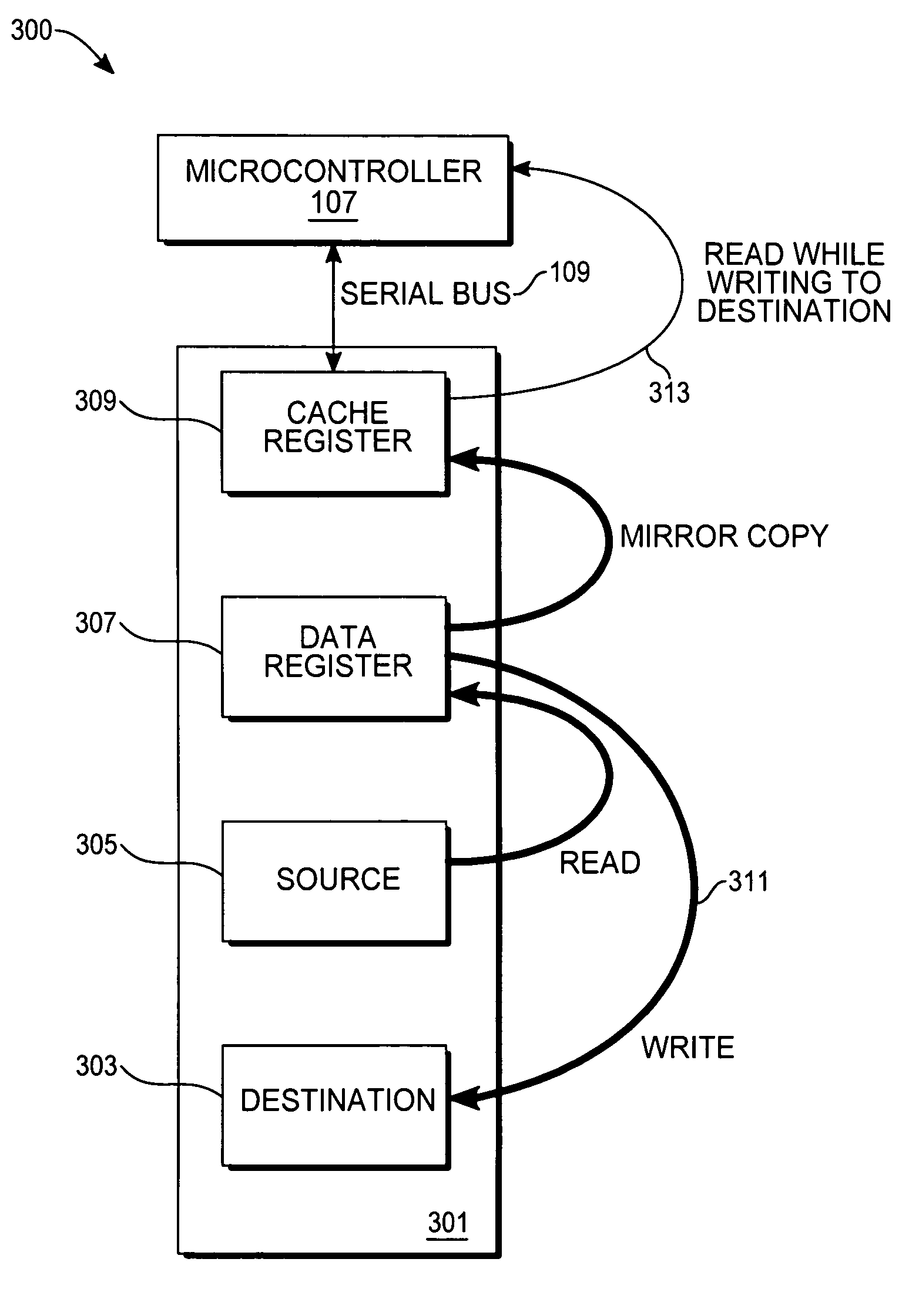
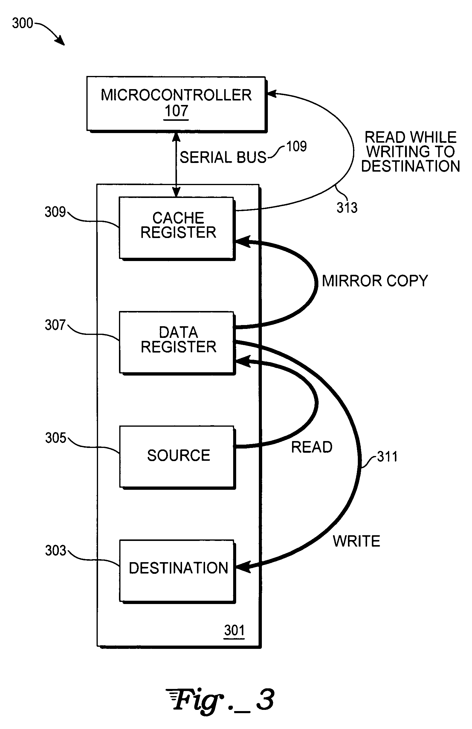
[0025]With respect to FIG. 3, a block diagram of a system 300 for performing a simultaneous external read operation during an internal programming operation in a flash device is shown. FIG. 3 includes a flash memory device 301, a destination address location 303, a source address location 305, a data register 307, and a cache register 309. A state machine (not shown), which may, for example, be co-located on an integrated circuit chip containing the flash memory device 301, is designed to control and carry out the routine, described infra.

[0026]In one embodiment, the flash memory device 301 is a NAND flash memory device. Alternatively, the flash memory device 301 could be based on either NOR or AND logic devices. Once a copy-back operation command has been asserted, data from the source address location 305 are read into the data register 307. The data read into the data register 307 may be, for example, an entire page of data. The page size, in one embodiment, consists of 256 byte ...


PUM


Abstract

A system and method for performing a simultaneous external read operation during internal programming of a memory device is described. The memory device is configured to store data randomly and includes a source location, a destination location, a data register, and a cache register. The data register is configured to simultaneously write data to the destination and to the cache register. The system further includes a processing device (e.g., a microprocessor or microcontroller) for verifying an accuracy of any data received through electrical communication with the memory device. The processing device is additionally configured to provide for error correction if the received data is inaccurate, add random data to the data, if required, and then transfer the error-corrected and / or random data modified data back to the destination location.

Description

TECHNICAL FIELD[0001]The present invention relates to semiconductor memory devices. More particularly, the present invention relates to a system and method for performing a copy-back operation in a memory cell.BACKGROUND ART[0002]Semiconductor memory devices are typically classified into volatile memory devices and non-volatile memory devices. Volatile memory devices are subdivided into dynamic random access memories (DRAMs) and static random access memories (SRAMs). Non-volatile memory types include mask read-only memories (MROMs), programmable read-only memories (PROMs), erasable programmable read-only memories (EPROMs), and electrically erasable programmable read-only memories (EEPROMs). EEPROMs are increasingly used in system programming that requires continuous update or auxiliary memory devices. Particularly, flash EEPROMs are advantageous as mass storage devices because their integration density is high compared with conventional EEPROMs. Among the flash EEPROMs, a NAND-type ...

Claims


Application Information

Patent Timeline
Patent Type & Authority Patents(United States)
IPC IPC(8): G06F12/16G11C29/00G11C7/10G06F12/00
CPCG06F11/1068G06F12/0804G11C16/26G06F12/0859G06F2212/2022G11C16/102G06F12/00
Inventor ADUSUMILLI, VIJAYA P.TELECCO, NICOLATEHRANI, ABBAS S.
Owner ATMEL CORP
Why Eureka
Try Eureka