Packaging structure and method for super-thin optical fingerprint interception module

A technology of packaging structure and packaging method, applied in character and pattern recognition, instruments, computer parts, etc., can solve problems such as increased manufacturing cost, reduced production yield, and bulky optical mechanism parts.

Inactive Publication Date: 2007-09-12
LITE ON SEMICON
View PDF0 Cites 7 Cited by
  • Summary
  • Abstract
  • Description
  • Claims
  • Application Information

AI Technical Summary

Problems solved by technology

[0004] However, as can be seen from FIG. 1 and FIG. 2, the volume of the optical mechanism part of the packaging structure of the known

Method used


Image

  • Packaging structure and method for super-thin optical fingerprint interception module
  • Packaging structure and method for super-thin optical fingerprint interception module
  • Packaging structure and method for super-thin optical fingerprint interception module

Examples


Embodiment Construction

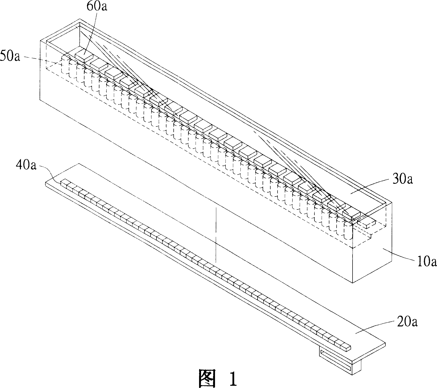
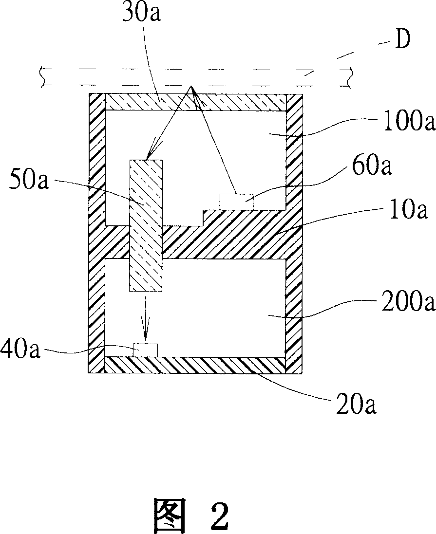
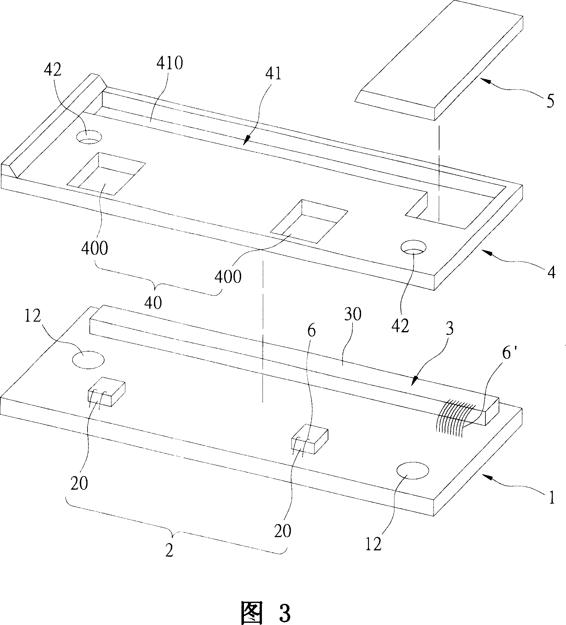
[0042] Please refer to FIG. 3 and FIG. 4 , which are respectively a three-dimensional exploded view and a three-dimensional assembled view of the packaging structure of the ultra-thin optical fingerprint capture module of the present invention. It can be seen from the figure that the present invention provides an ultra-thin optical fingerprint capture module packaging structure, which includes: a circuit board 1 , an image sensing module 2 , a light emitting module 3 and a packaging cover 4 .

[0043] Wherein, the image sensing module 2 and the light emitting module 3 are both electrically connected and arranged on the circuit board 1, and the image sensing module 2 may be composed of one or several CMOS image sensing chips 20 , in addition, the light emitting module 3 can also be composed of one or several light emitting components 30 .

[0044] Furthermore, the image sensing module 2 or the light emitting module 3 can be electrically connected to the circuit board 1 by wire-...


PUM


Abstract

The invention discloses an ultrathin optical fingerprint intercepting module packaging structure, comprising: a circuit board, an image sensing module, a lighting module and a packaging cover body, where the image sensing module and the lighting module are both arranged electrically on the circuit board; the packaging cover body is arranged on the circuit board and has a first opening unit for exposing the image sensing module and a second opening unit for exposing the lighting module. Therefore, the invention implements an ultrathin structure by reducing packaging structure volume and then can reduce the manufacturing cost and raise the product yield.

Description

technical field [0001] The invention relates to a packaging structure and a packaging method of an ultra-thin optical fingerprint interception module, in particular to a packaging structure and a packaging method which omit a complicated and difficult-to-assemble optical mechanism. Background technique [0002] Please refer to FIG. 1 and FIG. 2 , which are respectively an exploded perspective view and a side sectional view of a package structure of a conventional optical fingerprint capture module. It can be seen from the figure that the package structure of the known optical fingerprint capture module includes: a package case 10a, a circuit board 20a, a cover glass 30a, an image sensing component 40a, a lens component 50a and a light emitting component 60a. [0003] Wherein, the circuit board 20a and the upper cover glass 30a are respectively disposed on the upper and lower ends of the packaging case 10a, thereby creating upper and lower spaces 100a, 200a, the image sensing...

Claims


Application Information

Patent Timeline
IPC IPC(8): G06K9/00G06K9/20
Inventor 郑家驹张博政王明和
Owner LITE ON SEMICON
Why Eureka
Try Eureka