High-brightness LED and its making method

A technology of light-emitting diodes and manufacturing methods, which is applied to electrical components, circuits, semiconductor devices, etc., and can solve problems such as high difficulty, complicated process, and increased cost

Inactive Publication Date: 2007-10-17
HIGHLIGHT OPTOELECTRONICS
View PDF2 Cites 7 Cited by
  • Summary
  • Abstract
  • Description
  • Claims
  • Application Information

AI Technical Summary

Problems solved by technology

However, the processes of these technologies are not only complica

Method used


Image

  • High-brightness LED and its making method
  • High-brightness LED and its making method
  • High-brightness LED and its making method

Examples


Embodiment Construction

[0012] Preferred embodiments of the present invention will be described in more detail below with reference to the accompanying drawings.

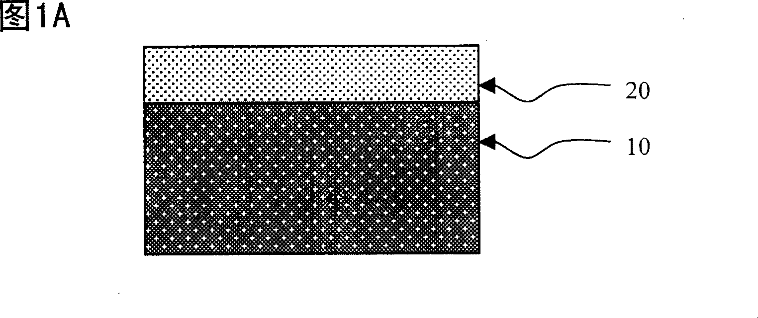
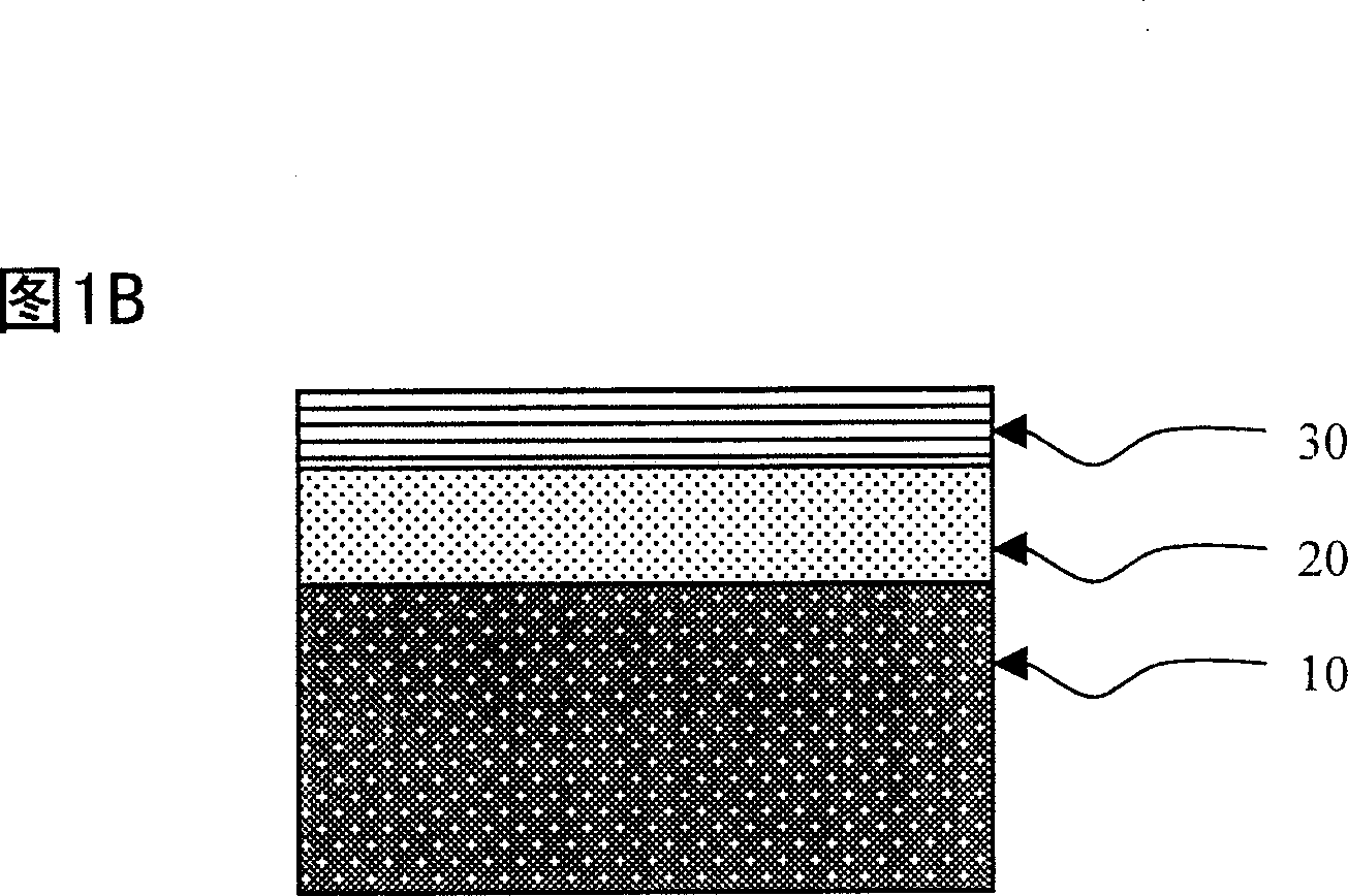
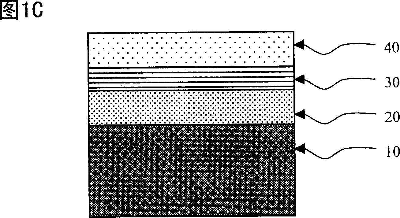
[0013] FIG. 1A to FIG. 1E are schematic diagrams showing implementation steps of a method for manufacturing a high-brightness light-emitting diode according to a specific embodiment of the present invention. As shown in FIG. 1A , first, using Liquid Phase Epitaxy (Liquid Phase Epitaxy, LPE) technology, on the substrate 10, grow crystal to form the first epitaxial layer 20, the thickness of the first epitaxial layer 20 is about 50 to 100 microns (μm), wherein the materials of the first epitaxial layer 20 and the substrate 10 are III-V group element compounds, for example, the material of the substrate 10 is gallium arsenide (GaAs), and the first epitaxial layer 20 The material used is aluminum gallium arsenide (AlGaAs). As shown in FIG. 1B, on the first epitaxial layer 20, a second epitaxial layer 30 is grown by metal organic vapor phase e...


PUM

PropertyMeasurementUnit
Thicknessaaaaaaaaaa
Thicknessaaaaaaaaaa

Abstract

The invention provides a high-brightness LED, comprising: a transparent substrate, which is formed by materials including aluminium arsenide gallium (AlxGa1-xAs); a luminescent layer, which grows up on the transparent substrate, and is formed by materials including aluminum phosphide gallium indium (AlGaInP); a window layer, which grows up on this luminescent layer, and is formed by materials including GaP; an upper electrode layer, which forms an ohm contact with the window layer; as well as a lower electrode layer, which forms an ohm contact with the transparent substrate, in which the x value in molecular formula AlxGa1-xAs of the transparent substrate material is set as a numerical value which makes the transparent substrate to have a transmissivity with high energy gap to the specific wavelength light sent by the luminescent layer.

Description

technical field [0001] The invention relates to a light-emitting diode and a manufacturing method thereof, in particular to a high-brightness light-emitting diode and a manufacturing method thereof, which can solve the problem that a substrate absorbs photons in the past. Background technique [0002] Light-emitting diode is a kind of semiconductor element, which is composed of p-type and n-type semiconductors. When passing a very small current, it can emit light due to the recombination of electrons and holes, which is different from the principle of ordinary incandescent bulbs or fluorescent tubes. However, when the light is generated inside the semiconductor, only a small part can be separated from the surface of the semiconductor to become a usable light source, and most of the light is reabsorbed inside the semiconductor. How to overcome this shortcoming is an extremely important issue. [0003] In the past, an aluminum gallium indium phosphide (AlGaInP) epitaxial lay...

Claims


Application Information

Patent Timeline
IPC IPC(8): H01L33/00H01L33/14H01L33/42
Inventor 倪英嘉倪国烟洪明正
Owner HIGHLIGHT OPTOELECTRONICS
Why Eureka
Try Eureka