Process for producing polycrystalline silicon bar

A manufacturing method, polysilicon technology, applied in the direction of polycrystalline material growth, chemical instruments and methods, silicon, etc., can solve the problems of reduced mechanical strength, reduced life characteristics, increased power costs, etc., to promote the promotion of crystal lattice arrangement, The effect of accelerating the crystal growth rate and improving the life characteristics

Inactive Publication Date: 2007-10-24
COSMOSS ENERGY JAPAN CO LTD +1
View PDF1 Cites 8 Cited by
  • Summary
  • Abstract
  • Description
  • Claims
  • Application Information

AI Technical Summary

Problems solved by technology

However, if the particle growth is promoted, the solidification time needs to be long, and in a decompressed argon atmosphere, there will be problems that the silica sintered body saggar used in the melting vessel, oxygen and carbon from the carbon saggar, and further The amount of carbon produced from the heater is also increased, dissolved in the silicon ingot, and the concentration of oxygen, carbon and other impurities will increase
[0009] As mentioned above, in the conventional method, there are the following problems: (1) In order to promote the particle growth of the polycrystalline silicon melt, a long solidification time is required, and the power cost of the production will increase.
(2) The concentration of oxygen, carbon and other impurities melted in the ingot for a long time will increase, resulting in a decrease in life characteristics
The content of these is to cause a decrease in mechanical strength or a decrease in life characteristics when the plate is thinned.

Method used


Image

  • Process for producing polycrystalline silicon bar
  • Process for producing polycrystalline silicon bar
  • Process for producing polycrystalline silicon bar

Examples


Embodiment 1

[0048] The following examples are given to illustrate the present invention more specifically, but these examples are of course illustrative and should not be limitedly interpreted.

[0049] (Example 1)

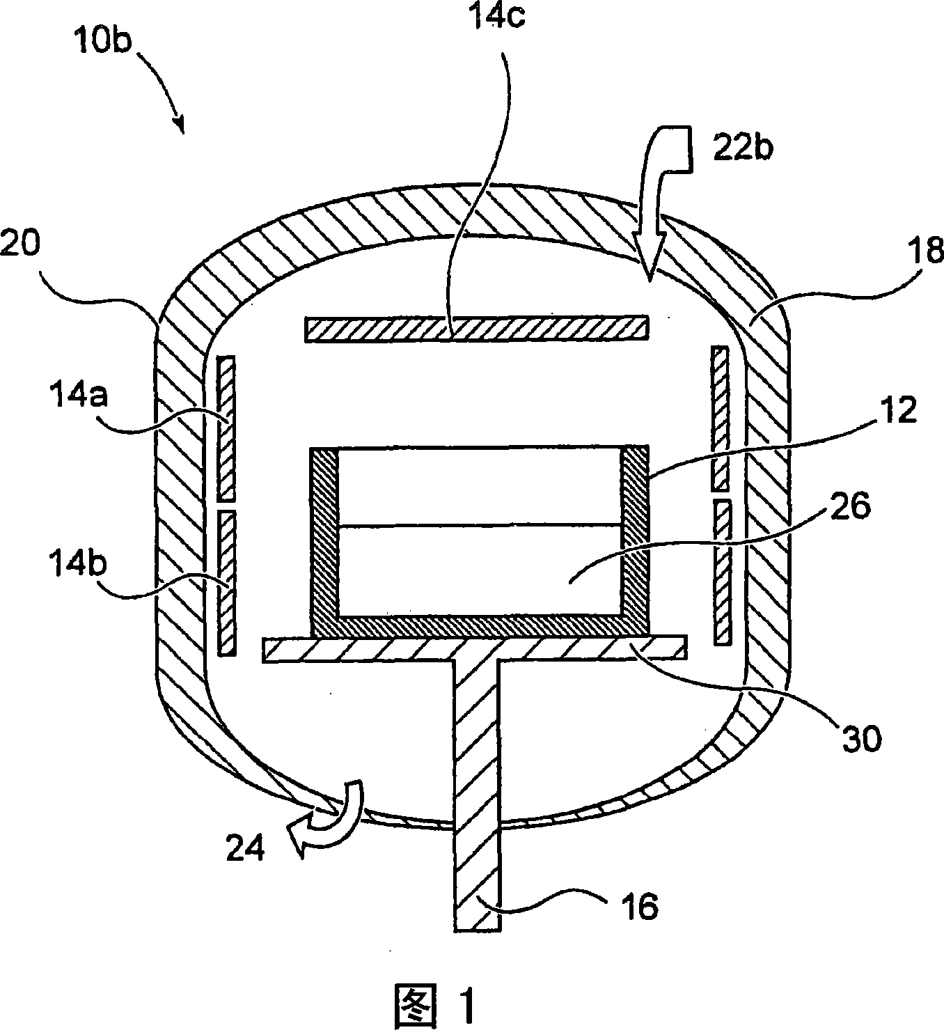
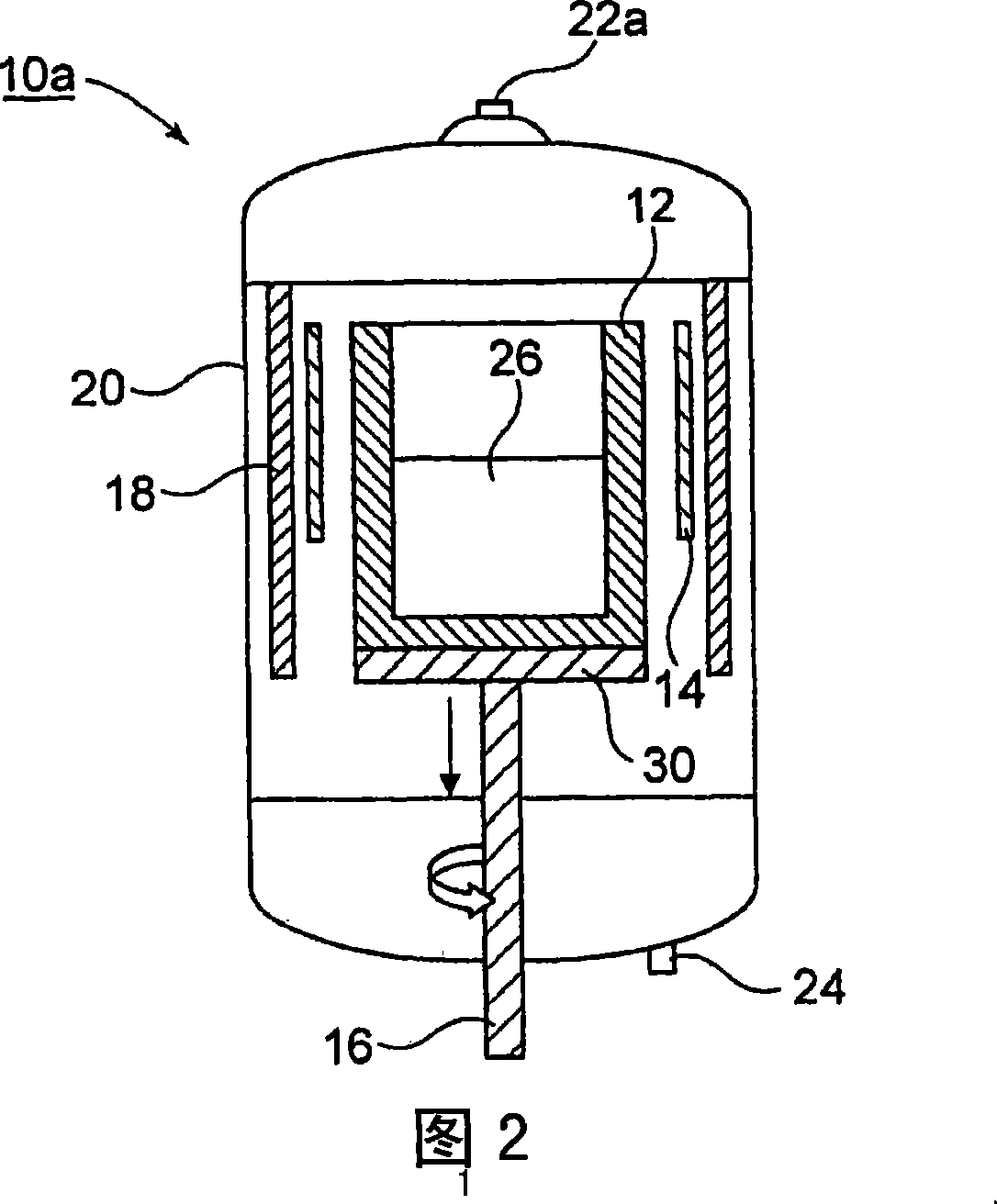
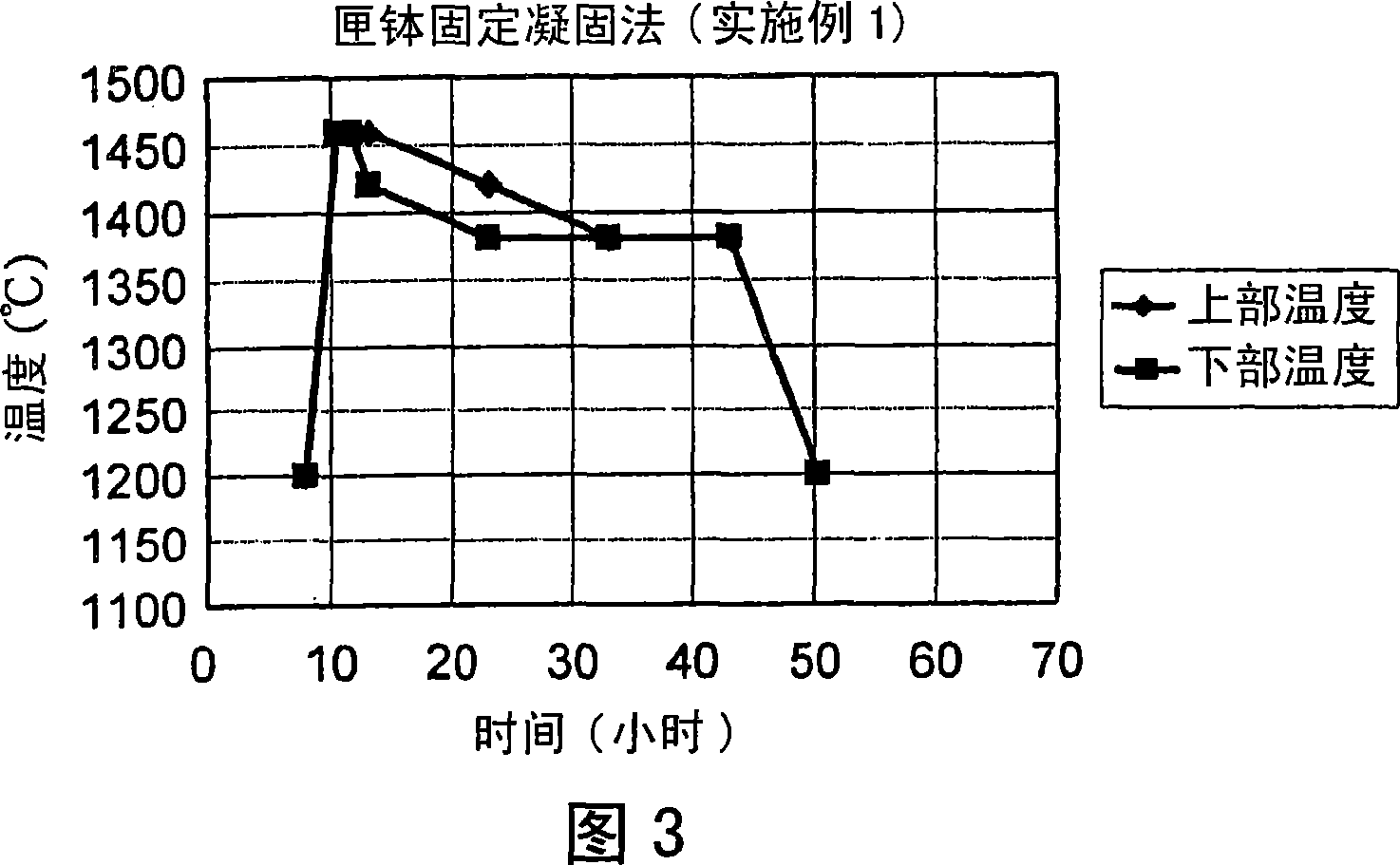
[0050] After coating the dry peeling material (high-purity silicon nitride powder) on the inner wall of the silica sintered body sagger (inner size 175mm×350mm), put high-purity silicon raw material into the melting furnace with the same structure as shown in Figure 1, to melt. In Example 1, silicon is melted at 1460°C in a state of slightly pressurized (500 Pa) with hydrogen gas in a melting furnace, and the temperature at the lower part of the sagger is lowered, and the temperature gradient between the upper and lower sides of the sagger is set. The temperature is lowered until the entire sagger reaches 1380°C, the silicon melt is solidified from the lower part of the sagger, and the temperature is further kept at 1380°C for 10 hours to produce polysilicon ingots. The tem...

Embodiment 2

[0054] An ingot was produced in the same manner as in Example 1 under a hydrogen atmosphere using the temperature profile diagram 5 at the same cooling rate of 4° C. / hr as in the melting in an argon atmosphere in Comparative Example 1.


PUM


Abstract

A process in which a polycrystalline silicon ingot improved in life time characteristics, which are correlated with the conversion efficiency of solar wafers, is inexpensively produced by the ordinary-pressure hydrogen-atmosphere melt method. In the process, the generation of oxygen and impurities in the silicon melt is inhibited and light-element impurities are removed through reaction or crystallization. Fine crystal grains can be grown at a high rate, and a high-purity polycrystalline silicon ingot having a crystal structure reduced in crystal defect can be grown. A silicon raw material is melted in an atmosphere of 100% hydrogen at ordinary pressure or an elevated pressure to prepare a silicon melt and simultaneously dissolve hydrogen in the silicon melt. The silicon melt containing hydrogen dissolved therein is solidified. Thereafter, the solid is held at a high temperature around the solidification temperature to grow silicon crystal grains in the solid phase and thereby obtain a polycrystalline silicon ingot.

Description

technical field [0001] The invention relates to a method for manufacturing polycrystalline silicon rods used in solar cells and the like. Background technique [0002] As a conventional method for producing polycrystalline silicon ingots for solar cells, a method of melting / solidifying a silicon raw material in an argon atmosphere under reduced pressure is generally known, as in the single crystal pulling method. A melting furnace used in this conventional method will be described with reference to FIG. 2 . FIG. 2 is a schematic explanatory diagram showing an example of a conventional melting furnace. In FIG. 2 , 10 a is a melting furnace, and has a sagger 12 , a heating device 14 for heating the sagger 12 , a support device 16 for placing the sagger 12 to rotate and ascend, a heat insulating material 18 , and a vacuum chamber 20 . The heat insulating material 18 is erected on the inner side of the side wall of the vacuum chamber 20 . Ambient gas, such as argon gas, is in...

Claims


Application Information

Patent Timeline
Patent Type & Authority Applications(China)
IPC IPC(8): C01B33/02
CPCC30B29/06C30B11/002C30B11/003
Inventor 木村义道酒井勇一
Owner COSMOSS ENERGY JAPAN CO LTD
Why Eureka
Try Eureka