Electronic device detecting system and electronic device detecting method

A technology of electronic equipment and detection system, applied in the field of detection system, can solve the problems of general products without structure, reduce quality, increase cost, etc., and achieve the effect of reducing product detection time

Inactive Publication Date: 2007-11-14
ACCTON TECHNOLOGY CORPORATION
View PDF0 Cites 1 Cited by
  • Summary
  • Abstract
  • Description
  • Claims
  • Application Information

AI Technical Summary

Problems solved by technology

[0004] When the inspector is performing the inspection, since one inspector usually observes many indicator lights at the same time, and the lights of the indicator lights will flicker, coupled with the influence of the surrounding environment, these factors often cause misjudgment by the inspector and affect the Product quality; in addition, because electronic equipment often needs to be matched with test fixtures for positioning and testing, it is more inconvenient for inspectors to observe the indicator light due to the influence of test fixtures, resulting in more misjudgments
Furthermore, the use of manual judgment not only increases the cost and reduces the quality, but also cannot test a large number of electronic devices at the same time, which makes the testing time of the product longer
[0005] It can be seen that the above-mentioned existing electronic equipment detection system and electronic equipment detection method obviously still have inconvenience and defects in product structure, detection method and use, and need to be further improved urgently.
In order to solve the above-mentioned problems, the relevant manufacturers have tried their best to find a solution, but no suitable design has been developed for a long time, and the general products do not have a suitable structure to solve the above-mentioned problems. This is obviously related. The problem that the industry is eager to solve

Method used


Image

  • Electronic device detecting system and electronic device detecting method
  • Electronic device detecting system and electronic device detecting method
  • Electronic device detecting system and electronic device detecting method

Examples


Embodiment Construction

[0069] In order to further explain the technical means and effects of the present invention to achieve the intended purpose of the invention, the specific implementation of the detection system for electronic equipment and the detection method for electronic equipment proposed according to the present invention will be described below in conjunction with the accompanying drawings and preferred embodiments. , structure, method, step, feature and effect thereof, detailed description is as follows.

[0070] The following will refer to the related drawings to illustrate an electronic device detection system and an electronic device detection method according to preferred embodiments of the present invention, wherein the same elements will be described with the same reference symbols.

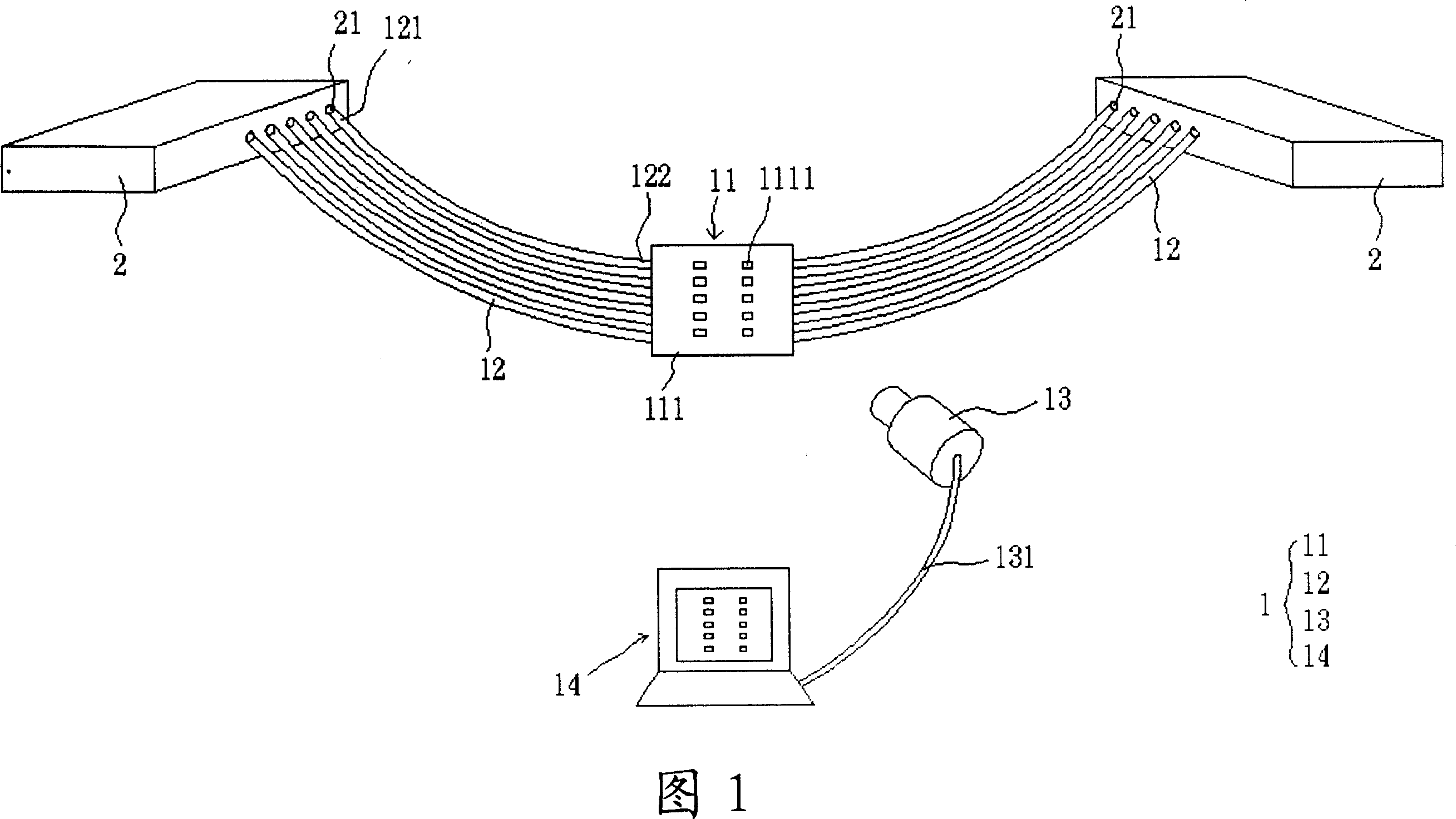
[0071] Please refer to FIG. 1 , which is a schematic diagram of a detection system for electronic equipment according to a first embodiment of the present invention. An electronic device detection s...


PUM


Abstract

The invention is about an electronic equipment detection systems and electronic equipment detection method. The electronic detection system equipment, electronic equipment has at least one indicator, a detection system includes modules on display, at least I. optical unit, a camera module and a data processing unit. I. Introduction optical modules are derived - and-derived cell-linking with the centralized show, beacons of light generated by entering into derivative-optical modules, derived from the end sent to the concentration showed that unit; camera modules display unit to concentrate on camera , and produce a video materials; data processing unit to receive image data. The electronic detection equipment, including the following steps: the indicator light will be guided to a centralized display unit; display unit to concentrate on the camera, and produce image data, and image data will be transmitted to a data processing unit. While this invention may be the majority of electronic devices for detection and detection products can reduce the time and improve the correct judgment rate and product quality.

Description

technical field [0001] The invention relates to a detection system and a detection method, in particular to a detection system and an electronic device capable of accurately detecting indicator lights on electronic equipment and simultaneously detecting a large number of electronic equipment, thereby shortening product detection time. The detection method of the equipment. Background technique [0002] Since the light emitting diode (light emitting diode, LED) began to be commercialized in the 1960s, due to its advantages of high shock resistance and long life, its application range has gradually spread in various electronic devices, as indicator lights, light sources or backlights. source etc. [0003] After the electronic devices with indicator lights are manufactured on the production line, functional testing of the electronic devices is required to ensure the quality of the products. Among them, the indicator light is a criterion for judging whether some functions of t...

Claims


Application Information

Patent Timeline
IPC IPC(8): G01R31/00G01R31/44
Inventor 卢信忠郑泽鸿王宜铭刘彦志
Owner ACCTON TECHNOLOGY CORPORATION
Why Eureka
Try Eureka