Shift register circuit and image display apparatus equipped with the same

A shift register and circuit technology, applied in static memory, digital memory information, instruments, etc., can solve the problems of gate line activation, malfunction, driving ability decline, etc., achieve fast rising and falling speed, prevent malfunction, The effect of preventing the decrease of driving ability

Inactive Publication Date: 2007-11-28
MITSUBISHI ELECTRIC CORP
View PDF1 Cites 57 Cited by
  • Summary
  • Abstract
  • Description
  • Claims
  • Application Information

AI Technical Summary

Problems solved by technology

[0019] As a result of the increase in the potential of the first node due to the above-mentioned leakage current and the clock signal, there is a problem of malfunction as follows: If the voltage between the gate and the source of the first transistor exceeds the threshold voltage, the first transistor that should be turned off is turned on. pass, the gate line is activated unnecessarily
In recent years, a display device using an amorphous silicon TFT (a-Si TFT) as a unit shift register of a gate line driver circuit has been widely used. However, a-Si TFT has the following problem: if the gate electrode is continuously biased voltage, the threshold voltage shifts, and its drive capability (capability to flow current) decreases
If this phenomenon continues, the output terminal will be in a floating state during the non-selection period, and since the potential of each gate line is unstable, malfunctions are likely to occur and the display quality will deteriorate.

Method used


Image

  • Shift register circuit and image display apparatus equipped with the same
  • Shift register circuit and image display apparatus equipped with the same
  • Shift register circuit and image display apparatus equipped with the same

Examples


Embodiment approach 1

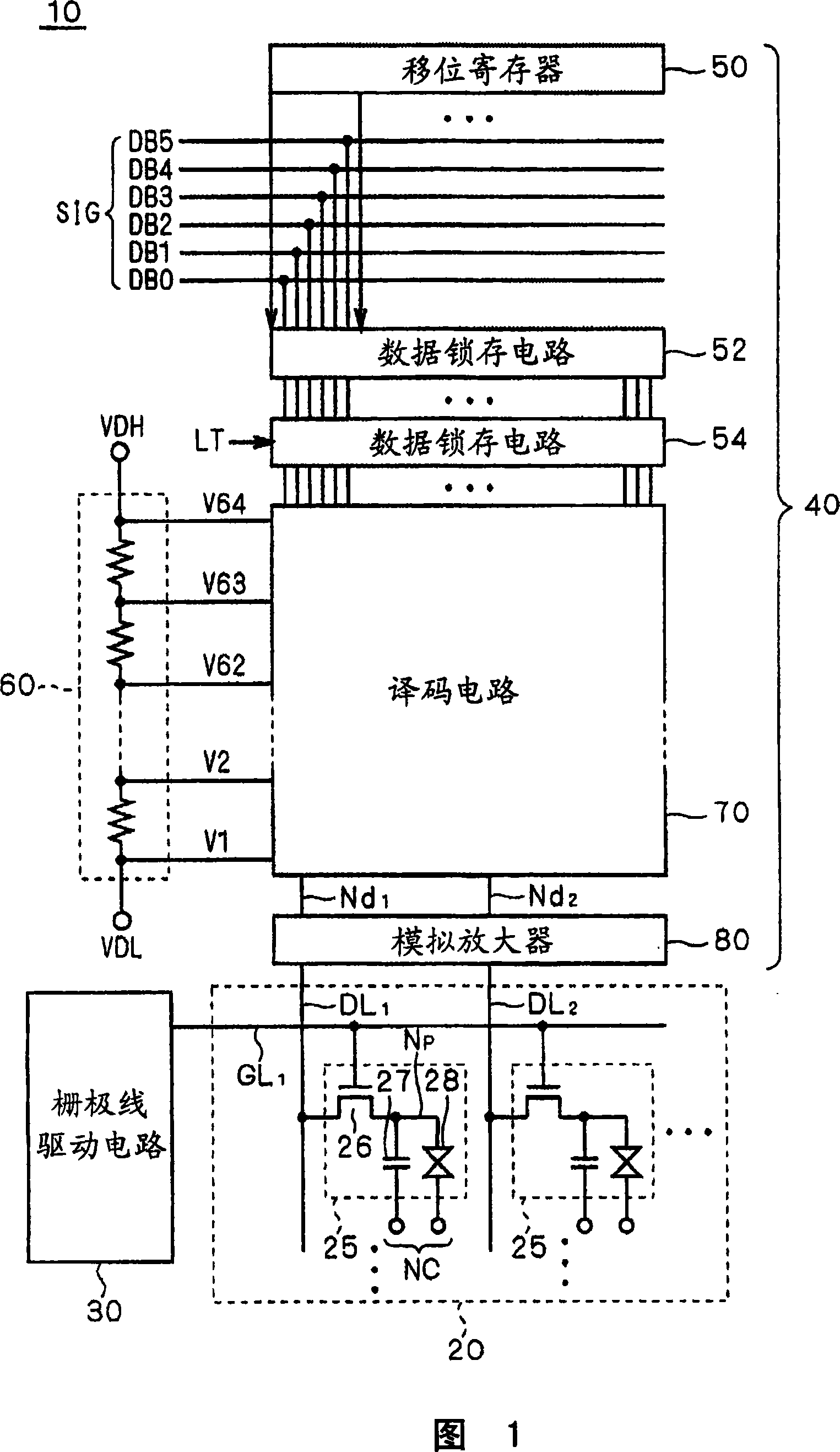
[0066] 1 is a schematic block diagram showing the structure of a display device according to Embodiment 1 of the present invention, and shows the overall structure of a liquid crystal display device 10 as a representative example of the display device.

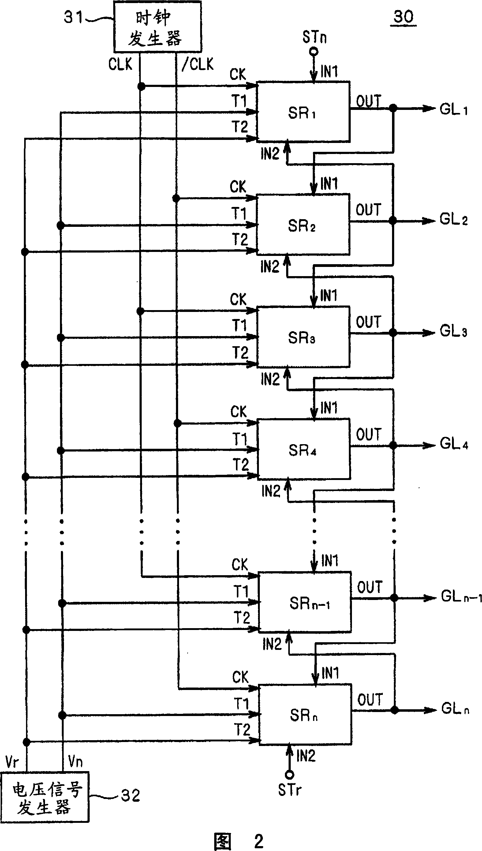
[0067] The liquid crystal display device 10 has a liquid crystal array section 20, a gate line driving circuit (scanning line driving circuit) 30, and a source driver 40. As will be understood from the following description, the bidirectional shift register of the embodiment of the present invention is mounted in the gate line drive circuit 30 and is formed integrally with the liquid crystal array section 20.

[0068] The liquid crystal array section 20 includes a plurality of pixels 25 arranged in a matrix. The gate line GL is arranged for each pixel row (hereinafter also referred to as "pixel line") 1 , GL 2 ...(Generally referred to as "gate line GL"), in addition, data lines DL are arranged for each pixel column (hereinafter a...

Embodiment approach 2

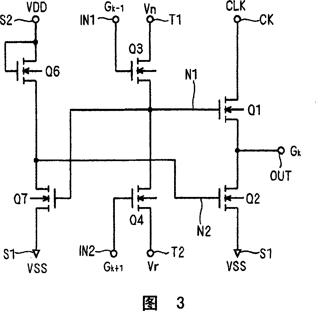
[0157] In the bidirectional shift register SR composed of the a-Si TFT of Embodiment 1 (FIG. 8), since the clock signal / CLK is input to the gate of the transistor Q2, it is possible to suppress the threshold voltage shift of the transistor Q2. The problem of gradual decline in its driving ability (the fourth problem mentioned above) arises. However, the threshold voltage of the transistor Q2 is not completely shifted, and there is a possibility that the threshold voltage gradually shifts when the clock signal / CLK repeatedly changes to the H level, and the above-mentioned problem may eventually occur. In the second embodiment, a unit shift register SR that can further suppress this problem is proposed.

[0158] FIG. 13 is a circuit diagram showing the structure of a unit shift register of the second embodiment. As shown in the figure, the source of the transistor Q2 is connected to the first clock terminal CK1. That is, one main electrode (drain) of the transistor Q2 is connected...

Embodiment approach 3

[0163] As explained using FIG. 10, in the bidirectional unit shift register SR of the first embodiment, the output signal (G k ) When rising, if the voltage between the gate and source of transistor Q5 V GS (Q5) When the threshold voltage Vth (Q5) is exceeded, a current (I(Q5)) flows from the node N1 to the output terminal OUT through the transistor Q5. As described above, normally, this current flows only slightly, and the level of the node N1 that affects the driving ability of the transistor Q1 is not reduced, so it is not a problem. However, the output load capacitance is large and the output When the signal rises slowly, the current I (Q5) flowing through the transistor Q5 may increase, and the driving capability of the transistor Q1 may decrease. In the third embodiment, a bidirectional unit shift register SR is proposed as a countermeasure.

[0164] FIG. 14 is a circuit diagram of a bidirectional unit shift register SR according to the third embodiment. In the unit shift re...


PUM


Abstract

Malfunction caused by leakage current of the transistor and shift in threshold voltage is prevented in the shift register in which the signal can be shifted bi-directionally. The bi-directional unit shift register includes a first transistor Q 1 for providing a first clock signal CLK to an output terminal OUT, a second transistor Q 2 for discharging the output terminal OUT based on a second clock signal, third and fourth transistors Q 3 , Q 4 for providing first and second voltage signals Vn, Vr complementary to each other to a first node, which is a gate node of the first transistor Q 1 , and a fifth transistor Q 5 connected between the first node and the output terminal OUT. The fifth transistor Q 5 is in an electrically conducted state based on the first clock signal CLK when the gate of the transistor Q 1 is at L (Low) level.

Description

Technical field [0001] The present invention relates to a shift register circuit composed only of field effect transistors of the same conductivity type used in, for example, a scanning line driver circuit of an image display device, and more particularly to a bidirectional shift register capable of reversing the direction of signal shift . Background technique [0002] In image display devices such as liquid crystal display devices (hereinafter referred to as "display devices"), gate lines (scanning lines) are provided in accordance with pixel rows (pixel lines) of a display panel in which a plurality of pixels are arranged in a matrix, and the display The gate lines are sequentially selected and driven within a period of one horizontal period of the signal, thereby enabling the display image to be updated. In this way, as a gate line driver circuit (scanning line driver circuit) for sequentially selecting and driving pixel lines, that is, gate lines, a shift register that perfo...

Claims


Application Information

Patent Timeline
Patent Type & Authority Applications(China)
IPC IPC(8): G09G3/36G09G3/20
CPCG09G3/3677G09G3/20G11C19/28G11C19/184G09G3/36G11C19/00
Inventor 飞田洋一
Owner MITSUBISHI ELECTRIC CORP
Why Eureka
Try Eureka