Semiconductor device and method for manufacturing the same, liquid crystal television, and EL television

a semiconductor device and semiconductor technology, applied in semiconductor devices, photomechanical treatment, instruments, etc., can solve the problems of reduced yield, reduced throughput, and difficulty in executing light-exposure treatment on a large-sized substrate at once for the photolithography device used for a photolithography step, so as to enhance the usability of materials

Inactive Publication Date: 2005-09-08
SEMICON ENERGY LAB CO LTD
View PDF10 Cites 41 Cited by
  • Summary
  • Abstract
  • Description
  • Claims
  • Application Information

AI Technical Summary

Benefits of technology

[0010] The present invention is made in view of the foregoing problems, and it is an object of the invention to provide a new method for forming a film pattern in which usability of a material is enhanced with the small number of steps.
[0011] In addition, it is an object of the invention to provide a method for manufacturing a semiconductor device having a semiconductor element with a minute structure which can reduce a cost and improve throughput with the small number of steps and a reduction of a raw material, and a method for manufacturing a liquid crystal television and an EL television.
[0045] Furthermore, since the light energy of the laser light is converted to heat energy by the light absorption layer and the heat energy is used, a film pattern having a very minute shape which exceeds the diffraction limit can be formed depending on thermal conductivity of the light absorption layer. Therefore, the minute film pattern formed by using a droplet discharging method can be processed, and thus, a semiconductor element having a minute structure can be formed. In addition, since a semiconductor element in which W / L is increased with minute structure can be formed, a semiconductor device having high driving capacity can be manufactured at low cost and a high throughput or yield. Furthermore, a semiconductor device such as a high integrated circuit or a display device having a high aperture ratio, and a liquid crystal television and an EL television having the semiconductor device can be manufactured at low cost and a high throughput or yield by using the minute semiconductor element.

Problems solved by technology

However, in a step of forming a film pattern using a conventional photolithography step, there is a problem that throughput is reduced due to a number of steps of forming a mask pattern, as well as wasting most parts of the material of a film pattern and a resist.
In addition, a photolithography device used for a photolithography step has difficulty in performing light-exposure treatment to a large-sized substrate at once.
Therefore, in a method for manufacturing a semiconductor device using a large-sized substrate, there is a problem that a yield is reduced since a plurality of light exposing times are required and unconformity with an adjacent pattern is generated.
However, in this case, the composition of the discharging solution is attached, dried and solidified at the end of the discharge opening and clogging or the like is generated.
Thus, it is difficult to continuously and stably discharge a certain amount of discharge solution.
Consequently, there is a problem that throughput or a yield of a semiconductor device formed from the semiconductor element is deteriorated.

Method used


Image

  • Semiconductor device and method for manufacturing the same, liquid crystal television, and EL television
  • Semiconductor device and method for manufacturing the same, liquid crystal television, and EL television
  • Semiconductor device and method for manufacturing the same, liquid crystal television, and EL television

Examples


embodiment mode 1

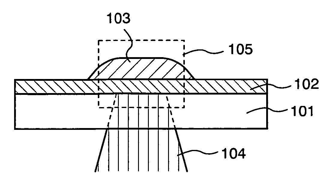
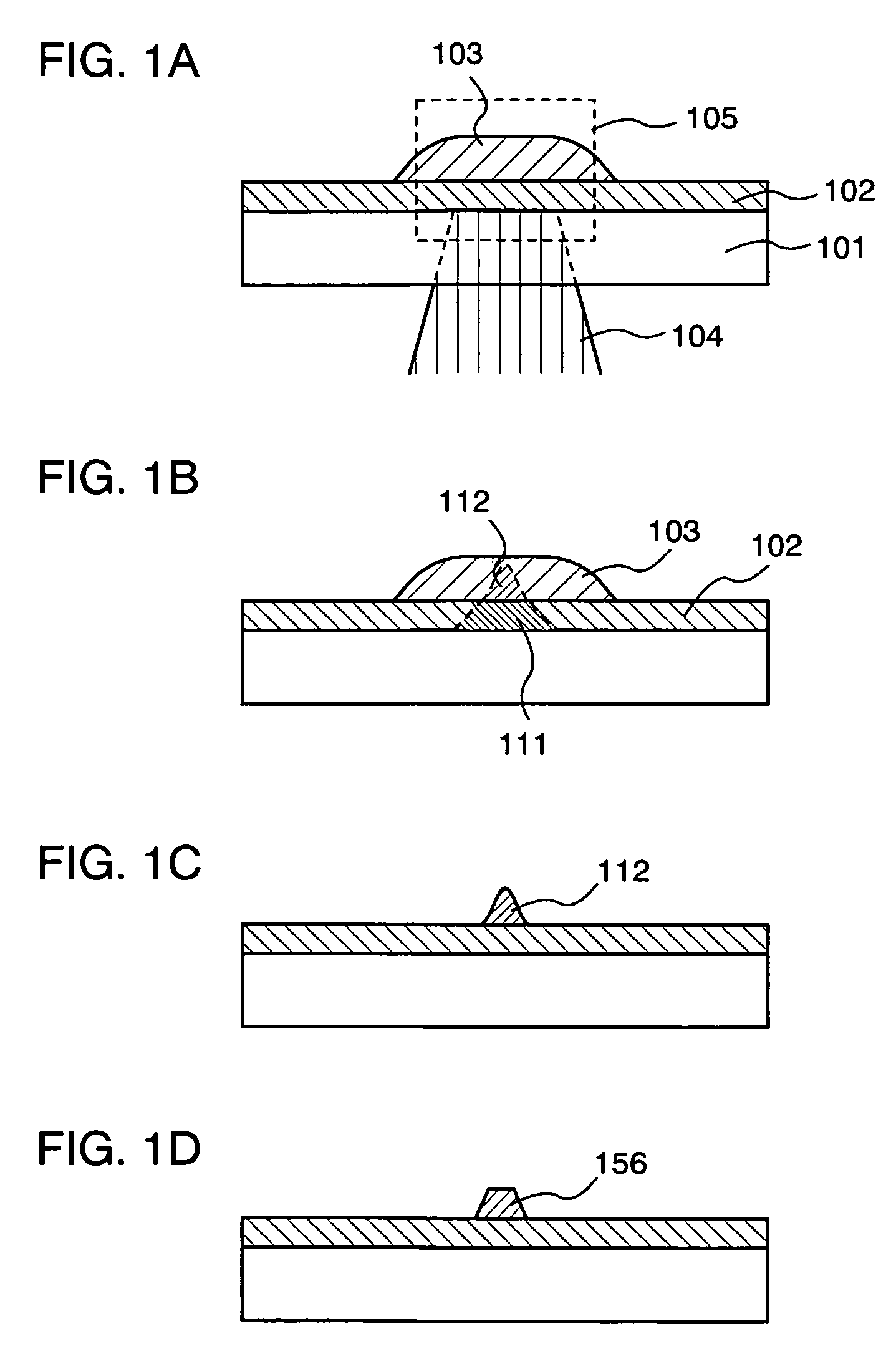
[0092] In this embodiment mode, a step of forming a film pattern using heat energy generated by absorbing light energy of laser light in a light absorption layer is described with reference to FIGS. 1A to 1D and FIGS. 8A to 8D.

[0093] As shown in FIG. 1A, a light absorption layer 102 is formed over a substrate 101, then, a solution 103 is applied or discharged over the light absorption layer 102.

[0094] A light-transmitting substrate is used as the substrate 101. Typically, a glass substrate, a quartz substrate, a plastic substrate having heat resistance which can withstand a processing temperature of a post-step and having light-transmitting properties or the like can be used. In addition, when the substrate 101 is a glass substrate, a large-area substrate of 320 mm×400 mm, 370 mm×470 mm, 550 mm×650 mm, 600 mm×720 mm, 680 mm×880 mm, 1000 mm×1200 mm, 1100 mm×1250 mm, 1150 mm×1300 mm or the like can be used. A quartz substrate is used here as the substrate 101.

[0095] Note that, in t...

embodiment mode 2

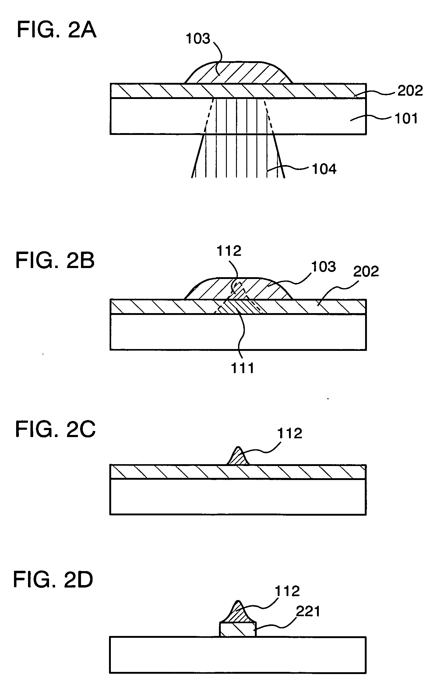
[0138] In this embodiment mode, a method for forming a film pattern when a light absorption layer 102 is formed from a conductive material and a solution in which conductors are dissolved or dispersed in a solvent is used for a solution 103 in Embodiment Mode 1 is described with reference to FIGS. 2A to 2D.

[0139] As shown in FIGS. 2A and 2B, as well as in Embodiment Mode 1, a solution 103 is applied or discharged over a light absorption layer 202 to form a first film pattern 112 in which part of the solution is baked by heat of laser light. Here, a tungsten film is formed as the light absorption layer 202 by using a tungsten target and an argon gas with a sputtering method. A silver (Ag) paste is used as the solution 103. A conductive layer containing silver as a main component is formed as the first film pattern 112. Thereafter, the unmodified solution 103 is removed.

[0140] Next, as shown in FIG. 2C, the light absorption layer 202 is etched by using a first film pattern 112. As a...

embodiment mode 3

[0143] In this embodiment mode, a step for forming a mask pattern with laser light and forming a film pattern with the mask pattern is described with reference to FIGS. 3A to 3D.

[0144] As shown in FIG. 3A, an insulating film 301 is formed over a substrate 101 to form a light absorption layer 202 over the insulating film. The insulating film 301 is used as an etching stopper; thus, silicon oxide, silicon nitride or the like is used. A conductive film having light-shielding properties with conductivity is used as the light absorption layer 202.

[0145] Next, a solution 302 is discharged over the light absorption layer. A thermosetting material or a thermoplastic material is used as a material of the solution. Polyimide which is a thermosetting material is used here as the solution 302. Then, the light absorption layer 202 is irradiated with laser light 104 from beneath the substrate 101. As a result, as shown in FIG. 3B, a heated region 311 is formed in part of the light absorption la...


PUM

PropertyMeasurementUnit
wavelengthaaaaaaaaaa
widthaaaaaaaaaa
quantum sizeaaaaaaaaaa

Abstract

An object of the present invention is to provide a method for manufacturing a semiconductor device having a semiconductor element capable of reducing a cost and improving a throughput with a minute structure, and further, a method for manufacturing a liquid crystal television and an EL television. According to one feature of the invention, a method for manufacturing a semiconductor device comprises the steps of: forming a light absorption layer over a substrate, forming a first region over the light absorption layer by using a solution, generating heat by irradiating the light absorption layer with laser light, and forming a first film pattern by heating the first region with the heat.

Description

BACKGROUND OF THE INVENTION [0001] 1. Field of the Invention [0002] The present invention relates to a semiconductor device formed by using a droplet discharge method, typified by an ink-jet method and a manufacturing method thereof. [0003] 2. Description of the Related Art [0004] Conventionally, a so-called active matrix driving type display panel or a semiconductor integrated circuit including a semiconductor element typified by a thin film transistor (hereinafter also referred to as a “TFT”) over a glass substrate is manufactured by patterning various thin films through a light-exposure step (hereinafter referred to as a photolithography step) using a photo mask. [0005] In a photolithography step, after a resist is applied to an entire surface of a substrate to perform prebaking, ultraviolet ray or the like is irradiated through a photo mask, and thus, development is performed to form a resist pattern. Thereafter, a thin film (a film formed from a semiconductor material, an insul...

Claims


Application Information

Patent Timeline
Patent Type & Authority Applications(United States)
IPC IPC(8): G03F7/00H01L21/027
CPCH01L51/5237H01L27/1292H01L51/5281H10K50/841H10K50/8426H10K50/86
Inventor SHIROGUCHI, HIROKOYAMAMOTO, YOSHIAKI
Owner SEMICON ENERGY LAB CO LTD
Why Eureka
Try Eureka