

Differential Drive Circuit and Electronic Apparatus Incorporating the Same
- Summary
- Abstract
- Description
- Claims
- Application Information
AI Technical Summary
Benefits of technology
Problems solved by technology
Method used
Image

Examples
first embodiment
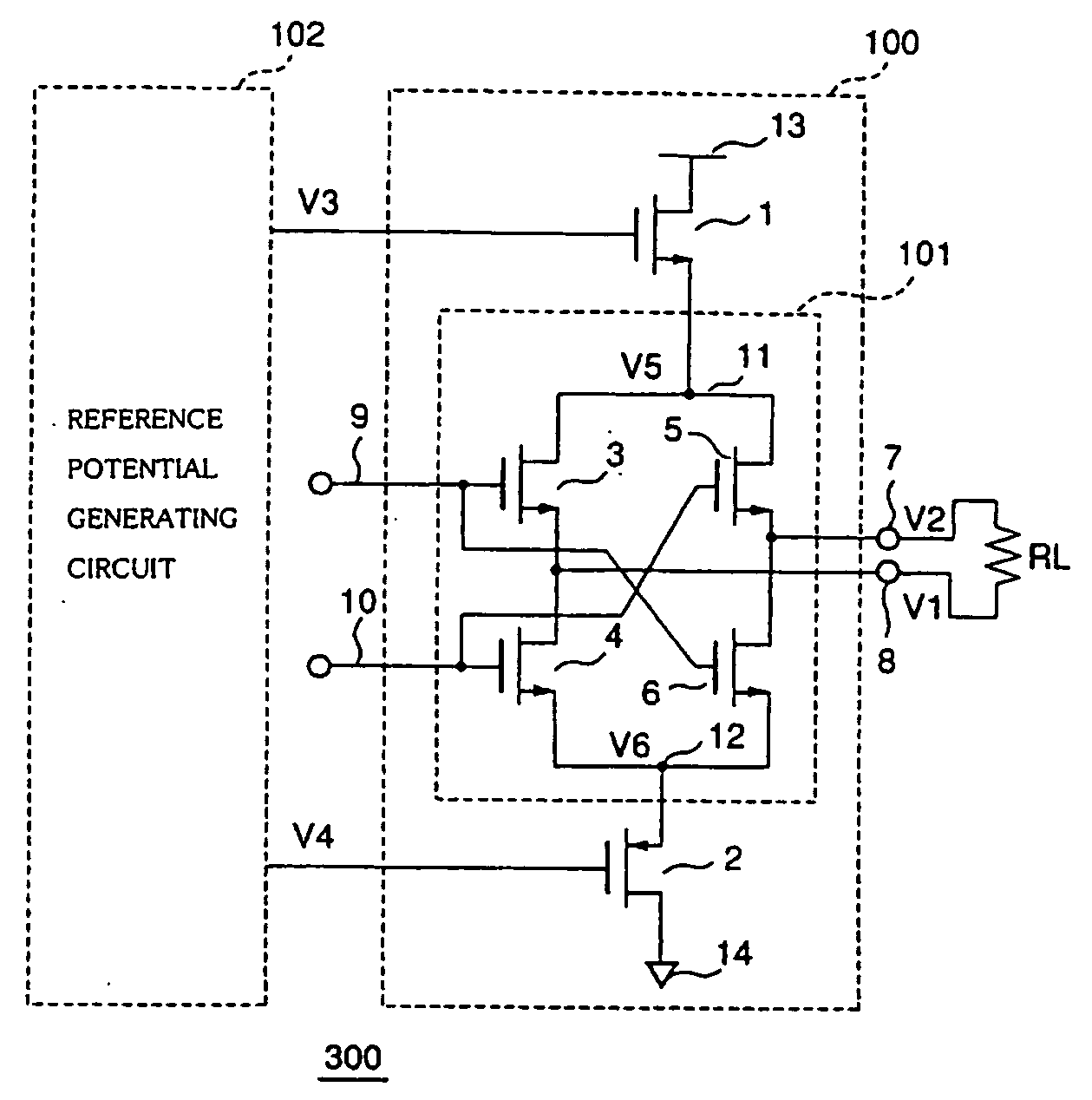
[0071]A first embodiment of a differential drive circuit for low voltage differential signals according to the present invention will be described by using FIG. 1. FIG. 1 is a circuit block diagram that describes a configuration of the differential drive circuit for low voltage differential signals of the present invention. A differential drive circuit 300 for low voltage differential signals of the present invention is constituted by an output circuit 100 in compliance with the LVDS interface standard (IEEE P1596, 3) and a reference potential generating circuit 102.
[0072]The output circuit 100 is constituted by a switching circuit 101 which receives differential signals inputted to and outputs current signals to a terminating resistor RL; a PMOS transistor 2 which is connected at its one end to a power supply potential 14 on the low potential side and at its other end to a node 12 in the switching circuit 101 and operates as a source follower; and an NMOS transistor 1 which is conn...
second embodiment
[0081]A second embodiment of a differential drive circuit for low voltage differential signals according to the present invention will be described by using FIG. 6. FIG. 6 is a circuit block diagram that describes a configuration of a high output differential drive circuit of the present invention. A differential drive circuit 300 for low voltage differential signals of the present invention is constituted by an output circuit 100, an emphasis circuit 300, and a bias circuit (not shown) for the circuits, for example, a reference potential generating circuit 102.
[0082]The output circuit 100 is a circuit described in FIG. 1. In the emphasis circuit 400, a drain of a PMOS transistor 61 is connected to a node 71 in a switching circuit for the emphasis circuit composed of MOS transistors, to which are inputted differential signals different from those inputted to the output circuit 100 and which outputs current signals. A source of the PMOS transistor 61 is connected to a power supply on...
PUM
 Abstract
Description
Claims
Application Information