Light Emitting Apparatus

a technology of light-emitting apparatus and light-emitting tube, which is applied in the direction of liquid/fluent solid measurement, volume metering, instruments, etc., can solve the problems of difficult to implement perfect white light, difficult to implement clear white light in a small package, and inability to uniformly mix colors, etc., to achieve reduced exterior size of the apparatus, reduced process trouble, and high luminance

Inactive Publication Date: 2008-07-10
SEOUL SEMICONDUCTOR
View PDF16 Cites 40 Cited by
  • Summary
  • Abstract
  • Description
  • Claims
  • Application Information

AI Technical Summary

Benefits of technology

[0018]In the light emitting apparatus of the present invention, the three-color light emitting device unit and the white light emitting device unit using blue LED chips and a fluorescent substance are constructed in one package to independently implement respective light with seven colors and white light. Thus, there is an advantage in that the apparatus can be applied to a variety of fields due to the implementation of various light. Further, since the two light emitting device units are simultaneously implemented, white light with high luminance can be obtained and the apparatus can be used as backlights for LCDs.
[0019]Further, the light emitting apparatus of the present invention can be used for not only indicators for use in keyboards, keypads and the like but also flashes for use in supplying a quantity of light required for photographing of camera chips provided in digital cameras and mobile terminals such as mobile phones and PDAs.
[0020]In addition, in the light emitting apparatus of the present invention, LEDs formed of different materials are constructed in one package by means of a simple method. Thus, there are advantages in that troublesomeness in a process can be reduced and the exterior size of the apparatus can be decreased.

Problems solved by technology

However, since the respective LED chips have different thermal or temporal characteristics, there are problems in that a uniformly mixed color cannot be implemented due to changes in a color tone according to usage environment, particularly, the occurrence of color spots, or the like.
However, since it is generally hard to achieve an optimal condition for mixture of three colors of light depending on the positions of the chips in view of the configuration of a package, it is difficult to implement perfect white light.
Since a color variation is generated due to differences in the light among the LED chips, it is difficult to implement a clear white color of light in a small package.
Further, since the respective LED chips have different thermal or temporal characteristics, there are disadvantages in that a uniformly mixed color cannot be implemented due to changes in a color tone according to usage environment, particularly, the occurrence of color spots, or the like, and in that luminance is not high.
Thus, since the luminance of white light is considerably low in the seven-color light emitting apparatus, it is not frequently used for emission of white light.
As described above, in a case where such a seven-color light emitting apparatus is applied to mobile phones and general electronic appliances, it is difficult to implement white light.
However, such prior arts have disadvantages in that there is troublesomeness in a process of manufacturing an additional white LED, and respective LED packages are separately manufactured and configured, resulting in an increased exterior size of an apparatus.

Method used


Image

  • Light Emitting Apparatus
  • Light Emitting Apparatus
  • Light Emitting Apparatus

Examples


first embodiment

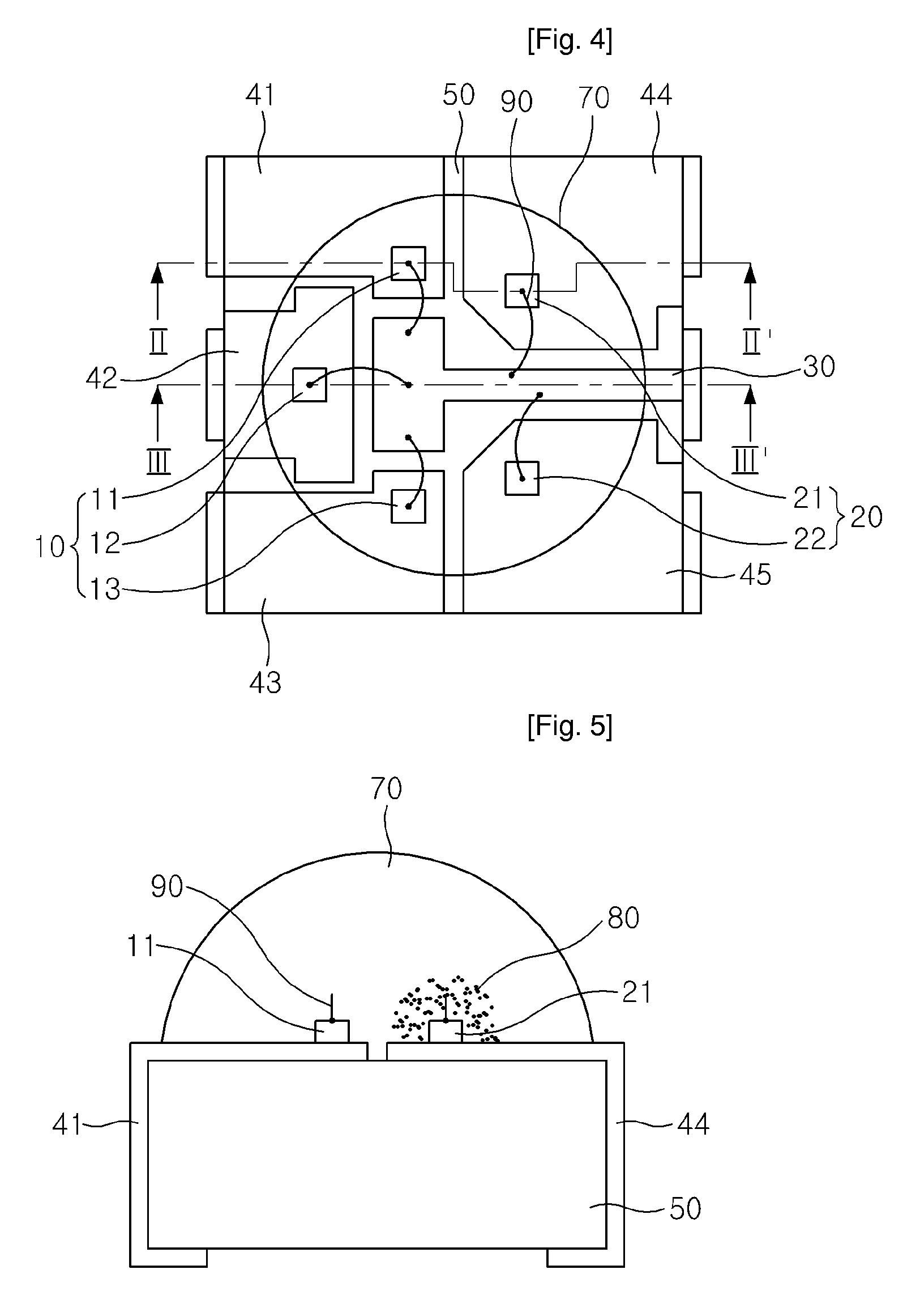
[0036]FIG. 4 is a schematic view showing a light emitting apparatus according to the present invention.

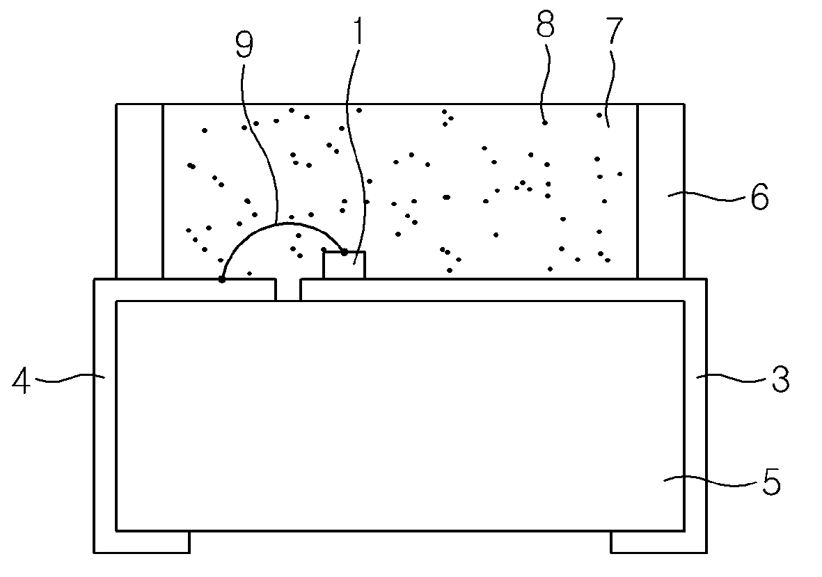
[0037]Referring to this figure, the light emitting apparatus comprises a substrate 50, electrodes 30 and 41 to 45 formed on the substrate 50, light emitting diode (LED) chips 11, 12 and 13 for respectively emitting red, green and blue light, and blue LED chips 21 and 22 on which a fluorescent substance is dotted. The light emitting apparatus further comprises a molding member 70 for encapsulating the LED chips on the substrate 50.

[0038]The electrodes 30 and 41 to 45 comprise a first electrode 30 connected in common to ends of the plurality of LED chips 11, 12, 13, 21 and 22, and second electrodes 41, 42, 43, 44 and 45 formed to respectively correspond to the plurality of LED chips 11, 12, 13, 21 and 22. The electrodes 30 and 41 to 45 formed on the substrate 50 may be formed by means of a printing technique or using an adhesive. The electrodes 30 and 41 to 45 are made of a metallic ...

second embodiment

[0047]FIG. 7 is a schematic view showing a light emitting apparatus according to the present invention.

[0048]Referring to this figure, the light emitting apparatus comprises a substrate 50, electrodes 30 and 41 to 45 formed on the substrate 50, light emitting diode chips 11, 12 and 13 for respectively emitting red, green and blue light, and blue LED chips 21 and 22 on which a fluorescent substance is dotted. The electrodes 30 and 41 to 45 comprise a first electrode 30 connected in common to ends of the plurality of LED chips 11, 12, 13, 21 and 22, and second electrodes 41, 42, 43, 44 and 45 formed to correspond respectively to the plurality of LED chips 11, 12, 13, 21 and 22. The plurality of LED chips 11, 12, 13, 21 and 22 are mounted on the second electrodes 41, 42, 43, 44 and 45, respectively, and are connected in common to the first electrode 30 through wires. Since this configuration is almost identical with that of the first embodiment, a detailed description thereof will be s...

third embodiment

[0055]FIG. 11 is a schematic view showing a light emitting apparatus according to the present invention.

[0056]Referring to this figure, the light emitting apparatus comprises a substrate 50, electrodes 30 and 41 to 45 formed on the substrate 50, light emitting diode chips 11, 12 and 13 for respectively emitting red, green and blue light, and blue LED chips 21 and 22 on which a fluorescent substance is dotted. The electrodes 30 and 41 to 45 comprise a first electrode 30 connected in common to ends of the plurality of LED chips 11, 12, 13, 21 and 22, and second electrodes 41, 42, 43, 44 and 45 formed to correspond respectively to the plurality of LED chips 11, 12, 13, 21 and 22. The light emitting apparatus further comprises an upper package 60 formed to surround the LED chips 11, 12, 13, 21 and 22 on the substrate 50. This configuration is almost identical with that of the second embodiment. However, the light emitting apparatus of the third embodiment further includes a partition 65...


PUM


Abstract

The present invention provides a light emitting apparatus comprising a three-color light emitting device unit including at least three light emitting diode (LED) chips for respectively emitting red, green and blue light; a white light emitting device unit including at least one blue LED chip with a fluorescent substance formed thereon; and a substrate provided with a first electrode connected in common to ends of the LED chips and second electrodes formed to correspond respectively to the LED chips. Further, the present invention provides a light emitting apparatus comprising a plurality of LED chips; a substrate provided with a first electrode connected in common to ends of the plurality of LED chips and second electrodes formed to correspond respectively to the plurality of LED chips; an upper package formed on the substrate to surround the plurality of LED chips and to have a partition crossing the first electrode at the center of the upper package; and a molding member that encapsulates the plurality of LED chips and is divided by the partition of the upper package.

Description

TECHNICAL FIELD[0001]The present invention relates to a light emitting apparatus, and more particularly, to a light emitting apparatus which can be used for not only indicators for use in keyboards, keypads and the like but also flashes for use in supplying a quantity of light required for photographing of camera chips provided in digital cameras and mobile terminals such as mobile phones and PDAs.BACKGROUND ART[0002]A light emitting diode (LED) refers to a device utilizing a phenomenon in which minority carriers (electrons or holes) injected by means of a p-n junction structure of a semiconductor are produced and light is emitted due to recombination of the carriers. LEDs include a red LED using GaAsP or the like, a green LED using GaP or the like, a blue LED using an InGaN / AlGaN double hetero structure, and the like.[0003]The LED has characteristics of low power consumption, a long lifespan, installation in a narrow space, and strong resistance against vibration. In recent years, ...

Claims


Application Information

Patent Timeline
Patent Type & Authority Applications(United States)
IPC IPC(8): H01L33/00H01L33/50
CPCH01L25/0753H01L33/50H01L2224/48091H01L2224/49113H01L2924/00H01L2924/00014G01F15/063G01F15/075H01L33/56H01L33/507H01L33/501H01L33/505
Inventor LEE, JAE HONG
Owner SEOUL SEMICONDUCTOR
Why Eureka
Try Eureka