Method for manufacturing electro-optical device and electro-optical device

A technology of electro-optical devices and manufacturing methods, applied in optics, identification devices, nonlinear optics, etc., capable of solving problems such as brightness shifts

Inactive Publication Date: 2007-12-12
SEIKO EPSON CORP
View PDF1 Cites 6 Cited by
  • Summary
  • Abstract
  • Description
  • Claims
  • Application Information

AI Technical Summary

Problems solved by technology

Therefore, according to the displayed color light components, a shift in luminance occurs

Method used


Image

  • Method for manufacturing electro-optical device and electro-optical device
  • Method for manufacturing electro-optical device and electro-optical device
  • Method for manufacturing electro-optical device and electro-optical device

Examples


Embodiment Construction

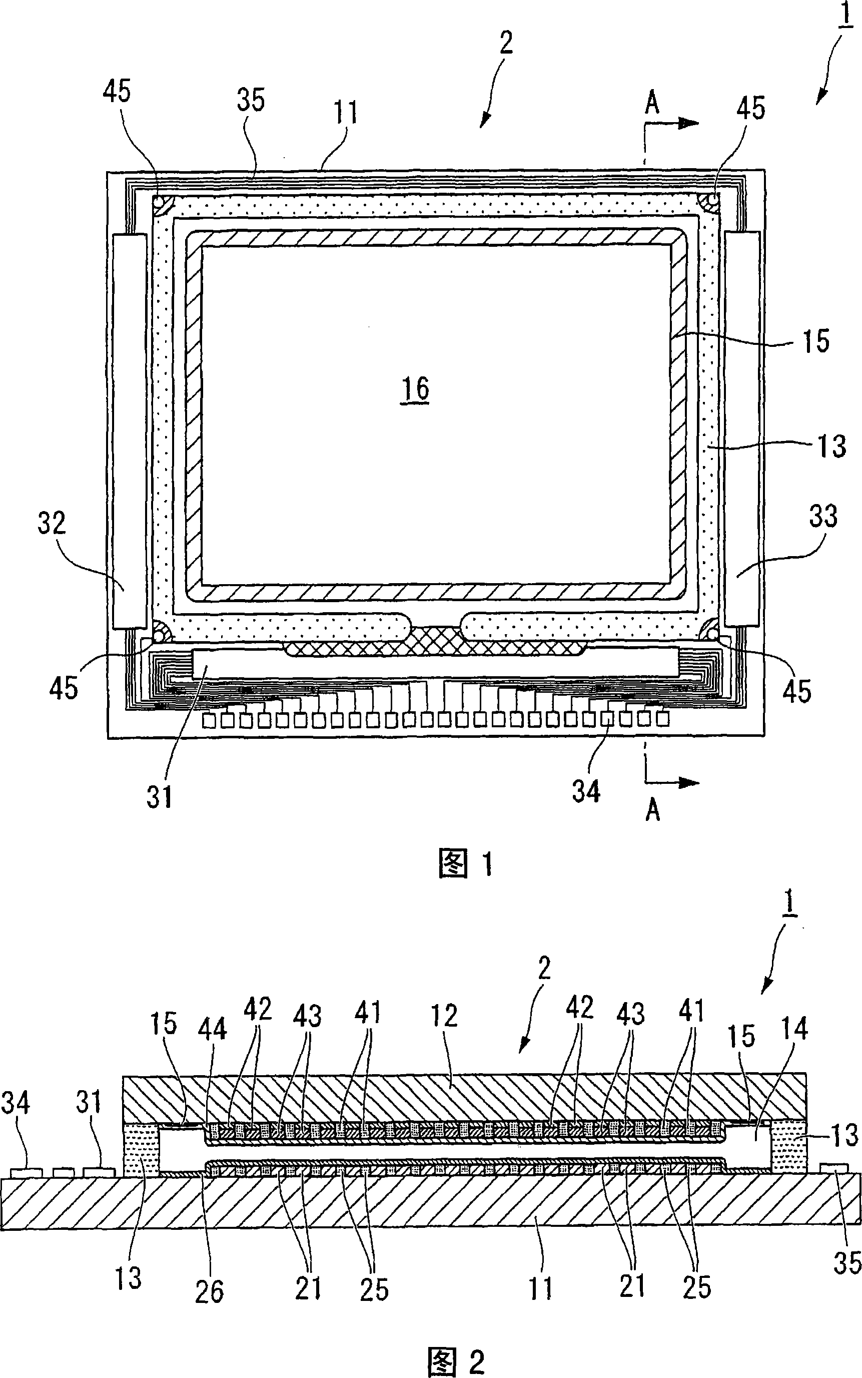
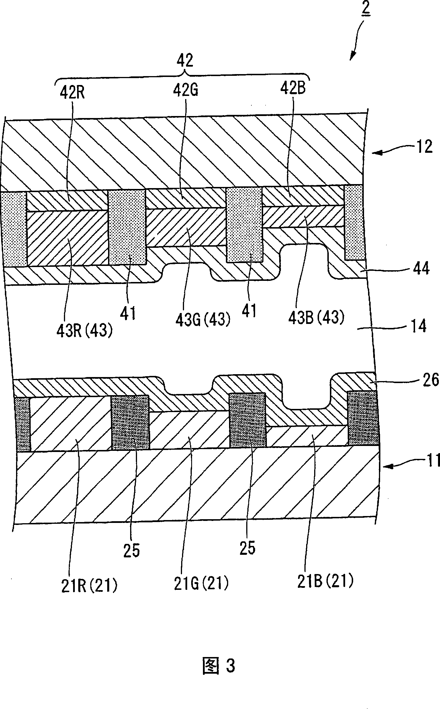
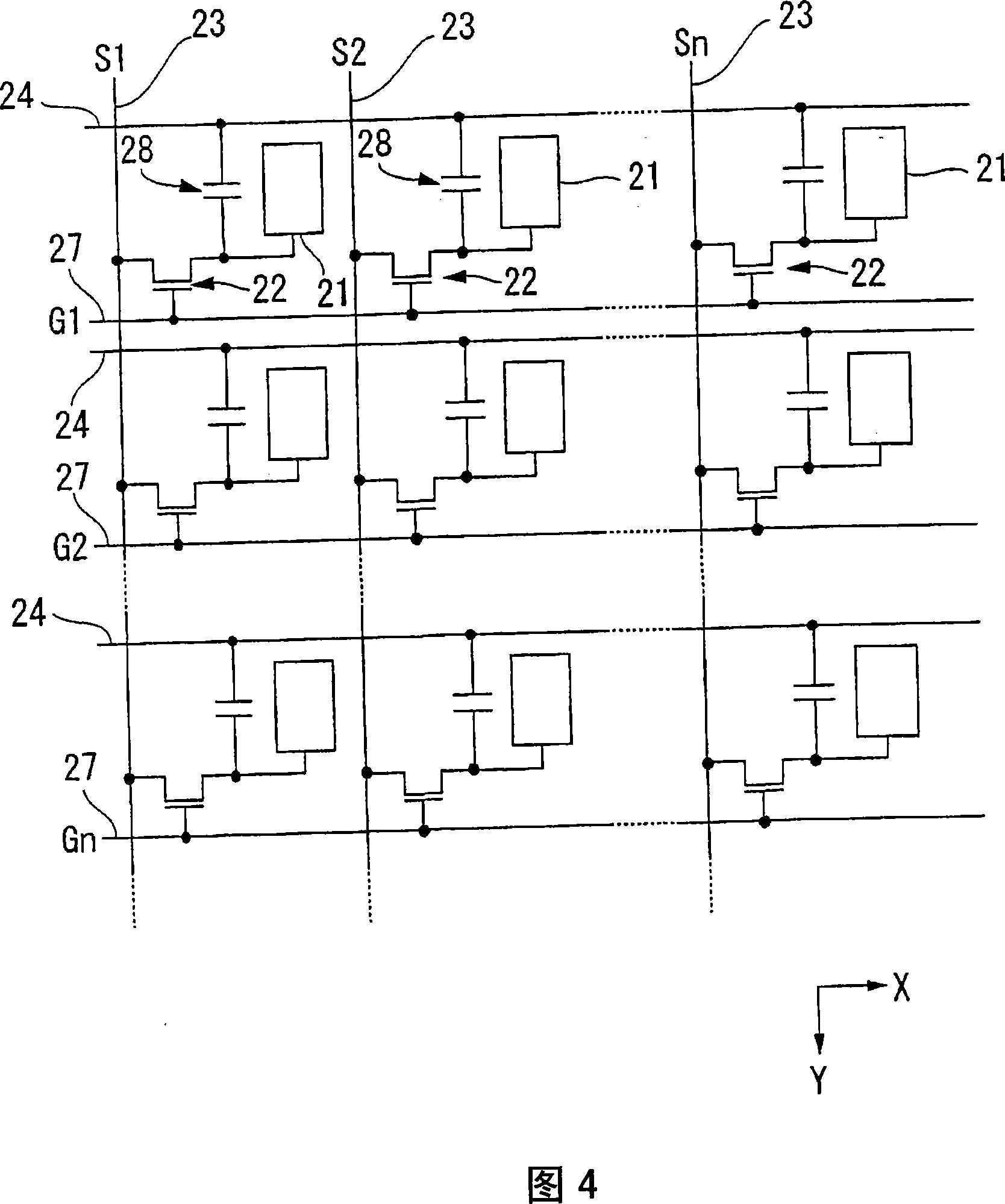
[0039] Hereinafter, an embodiment of a method of manufacturing an electro-optical device and an electro-optical device according to the present invention will be described with reference to the drawings. Here, FIG. 1 is a plan view of a liquid crystal device, FIG. 2 is a sectional view taken along the line A-A of FIG. 1, FIG. 3 is a partial enlarged view of FIG. 2, and FIG. 4 is an equivalent circuit diagram of the liquid crystal device. In addition, in each drawing used in the following description, in order to make each member recognizable, the dimension of each member is changed suitably.

[0040] The liquid crystal device (electro-optical device) 1 of this embodiment is a TFT active matrix type liquid crystal device using TFT (Thin Film Transistor: Thin Film Transistor) as a pixel switch. Furthermore, as shown in FIGS. 1 to 4 , the liquid crystal device 1 includes a liquid crystal panel 2 and polarizing plates (not shown) respectively arranged on the outer surfaces of the ...


PUM

PropertyMeasurementUnit
thicknessaaaaaaaaaa
thicknessaaaaaaaaaa
particle diameteraaaaaaaaaa

Abstract

A method of the invention comprises the following steps: a partition wall forming step for forming the partition wall (41) that divides the pixel area on the opposite substrate (12); and an opposite electrode forming step for respectively coating the opposite electrode forming material liquid (51) respectively in the areas divided by the partition wall (41) to form the opposite electrode (43); in the opposite electrode forming procedure the layer thickness of the opposite electrode (43) is set according to the wavelength strip of the light transmitting the corresponding arranged color filter layers (42R, 42G and 42B). Each color according to the displaying is provided, and the invention provides a method for manufacturing the electro-optical device which can be formed with transparent electrodes with different layer thickness and the electro-optical device.

Description

technical field [0001] The present invention relates to a method of manufacturing an electro-optical device such as a liquid crystal device and the electro-optical device. Background technique [0002] Conventionally, liquid crystal devices have been widely used as components for displaying image information in electronic devices such as notebook personal computers, mobile phones, and electronic notebooks. In such a liquid crystal device, a color filter substrate (counter substrate) is embedded for color display. The color filter substrate has colored layers of three colors such as R (red), G (green), and B (blue) arranged in a given pattern corresponding to pixels on a base material made of transparent glass. A transparent electrode for driving the liquid crystal layer and an alignment film for aligning liquid crystal molecules constituting the liquid crystal layer are formed. [0003] In such a color filter substrate, when light enters the transparent electrode, it is re...

Claims


Application Information

Patent Timeline
Patent Type & Authority Applications(China)
IPC IPC(8): G02F1/1362G02F1/1333G02F1/1337G02F1/133
CPCG02F1/133371G02F2001/133521G02F2203/055G02F2201/123G02F1/133516G02F1/13439G02F1/133521G02F1/1343G09F9/35
Inventor 野田洋一
Owner SEIKO EPSON CORP
Why Eureka
Try Eureka