Liquid crystal display device
A technology of liquid crystal display device and liquid crystal layer, which is applied in the direction of static indicators, nonlinear optics, instruments, etc., and can solve the problems of large thickness deviation of columnar spacers, deviation of resin film thickness, and degradation of display quality of liquid crystal display devices, etc. , to achieve the effects of less gap unevenness, reduced film thickness deviation, and superior display quality
- Summary
- Abstract
- Description
- Claims
- Application Information
AI Technical Summary
Problems solved by technology
Method used
Image

Examples
no. 1 approach
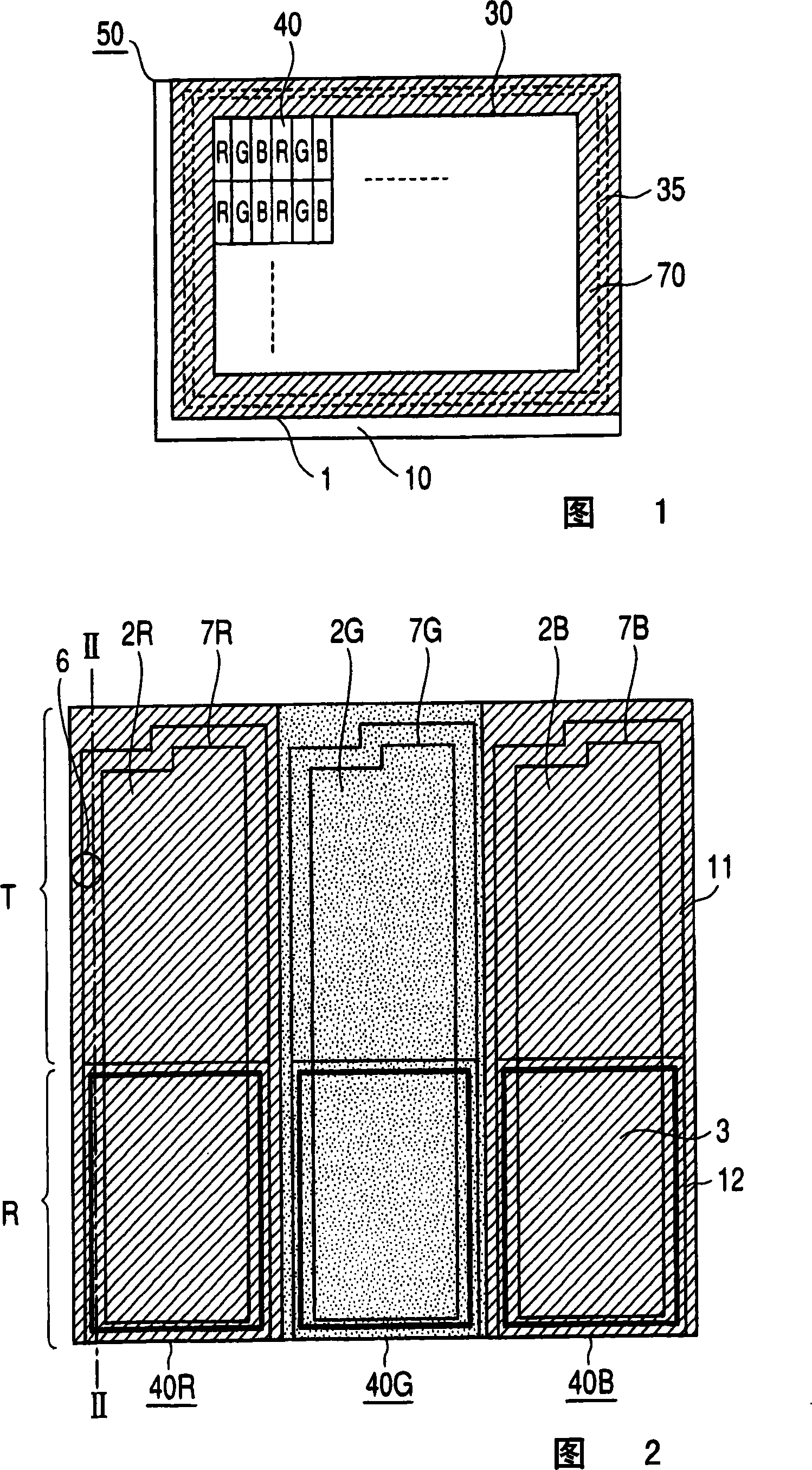
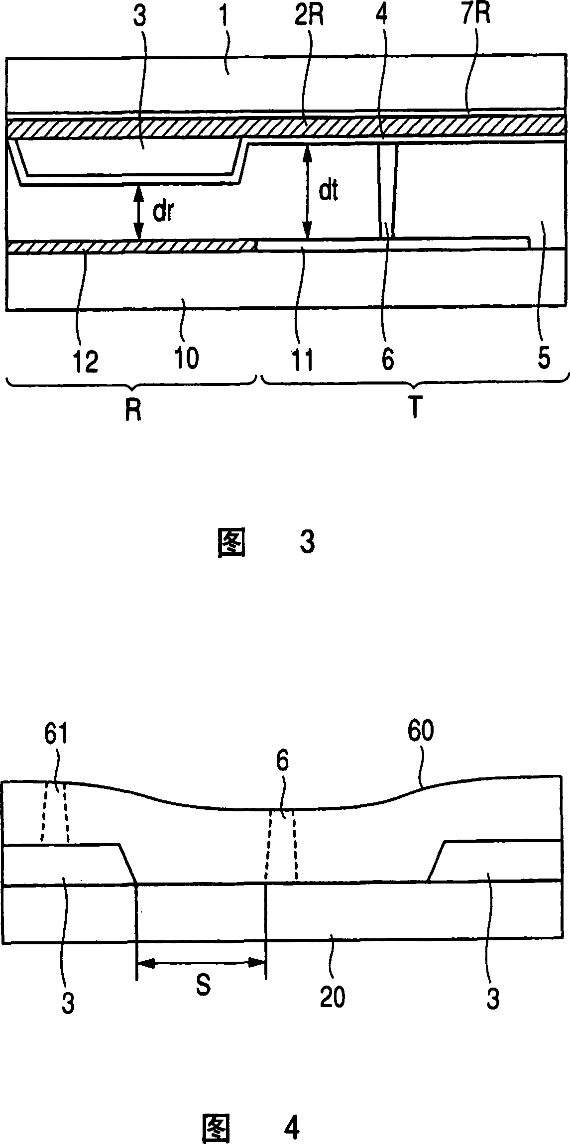
[0044] FIG. 1 is a plan view showing the outline of the liquid crystal display device in the first embodiment of the present invention. 2 is a plan view showing a pixel of the liquid crystal display device in the first embodiment, and FIG. 3 is a cross-sectional view of the pixel in FIG. 2 taken along the II-II section. In addition, in the following drawings, the same reference numerals denote the same or equivalent parts.
[0045] In FIG. 1, a liquid crystal panel 50 is composed of a color filter substrate 1 as a first substrate and an array substrate 10 as a second substrate that sandwich a liquid crystal layer 5. The display unit 30 is composed of a plurality of pixels 40 arranged in a matrix. A display portion peripheral light shielding film 70 is formed on the outer periphery of the display portion 30, and a sealing portion 35 in which a sealing material for sealing the liquid crystal layer 5 is formed is provided in the display portion peripheral light shielding film 70 area...
no. 2 approach
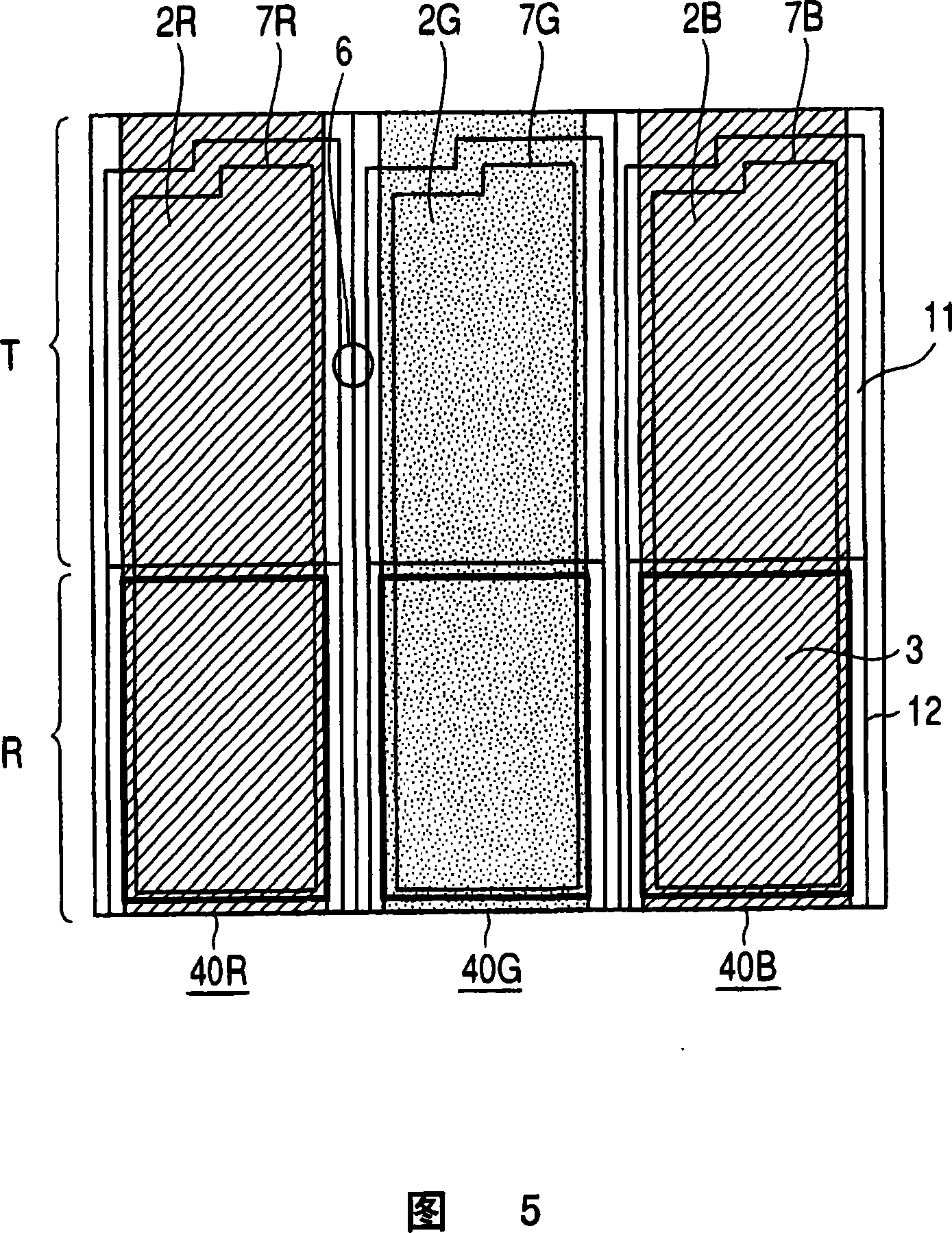
[0080] In the first embodiment, the case where the columnar spacer 6 is formed on the colored layer 2 where the protrusion 3 is not formed is described. However, as shown in FIG. The area where the colored layer 2 is formed forms a columnar spacer 6. Here, the colored layers 2R, 2G are not partially formed in the regions where the light-shielding films 7R, 7G are formed in the boundary portions of the left and right adjacent pixels 40R, 40G. In addition, the regions where the colored layers 2R, 2G, and 2B are not formed extend in stripes up and down. The columnar spacer 6 is formed in the area where the colored layers 2R and 2G are not formed. In addition, the columnar spacer 6 is arranged substantially in the center between the ends of the protrusions 3 of the pixels 40R and 40G adjacent to each other in the vertical direction.
[0081]In this embodiment, the columnar spacer 6 is arranged at the boundary between the pixels 40R and 40G adjacent to the left and right. However, the ...
no. 3 approach
[0083] In the first and second embodiments, as shown in FIGS. 2 and 5, the protrusions 3 formed on the color filter substrate 1 are formed as island-shaped isolated patterns in each pixel 40, but as As shown in FIG. 6, it may be formed in a stripe shape continuous through a plurality of pixels 40R, 40G, and 40B. Here, the transmissive display area T where the protrusion 3 is not formed at the boundary of the left and right adjacent pixels 40R and 40G, and the columnar spacer 6 is formed in the area where the light-shielding films 7R and 7G are formed. In addition, the columnar spacer 6 is arranged substantially in the center between the ends of the protrusions 3 of the pixels 40R and 40G adjacent to each other in the vertical direction.
[0084] In this embodiment, since the columnar spacer 6 is formed in the transparent display area T where the protrusion 3 is not formed, the gap dt of the transparent display area T is not affected by the step difference of the protrusion 3 or th...
PUM
| Property | Measurement | Unit |
|---|---|---|
| diameter | aaaaa | aaaaa |
Abstract
Description
Claims
Application Information
 - R&D
- Intellectual Property
- Life Sciences
- Materials
- Tech Scout
- Unparalleled Data Quality
- Higher Quality Content
- 60% Fewer Hallucinations
Browse by: Latest US Patents, China's latest patents, Technical Efficacy Thesaurus, Application Domain, Technology Topic, Popular Technical Reports.
© 2025 PatSnap. All rights reserved.Legal|Privacy policy|Modern Slavery Act Transparency Statement|Sitemap|About US| Contact US: help@patsnap.com