Semiconductor device and its manufacturing method

a technology of semiconductors and semiconductors, applied in semiconductor devices, electrical equipment, transistors, etc., can solve the problems of inability to manufacture a conventional one-layer gate type non-volatile memory, and achieve the effects of enhancing the reliability of both gate oxide films, reducing film thickness variation, and enhancing the reliability of high-voltage endurance gate oxide films

Inactive Publication Date: 2005-12-15
RICOH KK
View PDF4 Cites 0 Cited by
  • Summary
  • Abstract
  • Description
  • Claims
  • Application Information

AI Technical Summary

Benefits of technology

[0027] A second object of the present invention is offering a manufacturing method that can reduce film thickness variation of both a gate oxide film for the memory, and a gate oxide film for transistors, such that the reliability is improved, when forming a non-volatile memory and other transistors simultaneously.
[0036] According to the first manufacturing method, the semiconductor device of the present invention can be manufactured. Further, both the gate oxide film for the transistor and the gate oxide film for the memory can be formed by the once-oxidized film, enhancing the reliability of the both gate oxide films, and reducing film thickness variation.
[0043] According to the second manufacturing method, the semiconductor device of the present invention can be manufactured. Further, both the low voltage endurance gate oxide film for the low voltage transistor and the gate oxide film for the memory are formed by the once-oxidized film, enhancing the reliability of the both gate oxide films, and reducing film thickness variation.
[0044] Further, since the gate electrode for the low voltage transistor and the gate electrode for the high-voltage transistor are formed separately from the floating gate, silicide processing by tungsten silicide etc. of the gate electrode for the low voltage transistor and the gate electrode for the high-voltage transistor is facilitated.
[0052] According to the manufacturing method, the semiconductor device of the present invention can be manufactured. Further, both the low voltage endurance gate oxide film for the low voltage transistor and the gate oxide film for the memory are formed with the once-oxidized film, enhancing the reliability of both gate oxide films, and reducing film thickness variation. Further, the high voltage endurance gate oxide film for the high-voltage transistor is formed with the twice-oxidized film, enhancing the reliability of the high voltage endurance gate oxide film, and reducing film thickness variation, compared with the conventional technology.

Problems solved by technology

Further, since the control gate is formed on the first insulation film, being electrically separated from the semiconductor substrate, both positive and negative voltages can be applied to the control gate, which is impossible in a conventional one-layer gate type non-volatile memory.

Method used


Image

  • Semiconductor device and its manufacturing method
  • Semiconductor device and its manufacturing method
  • Semiconductor device and its manufacturing method

Examples


first embodiment

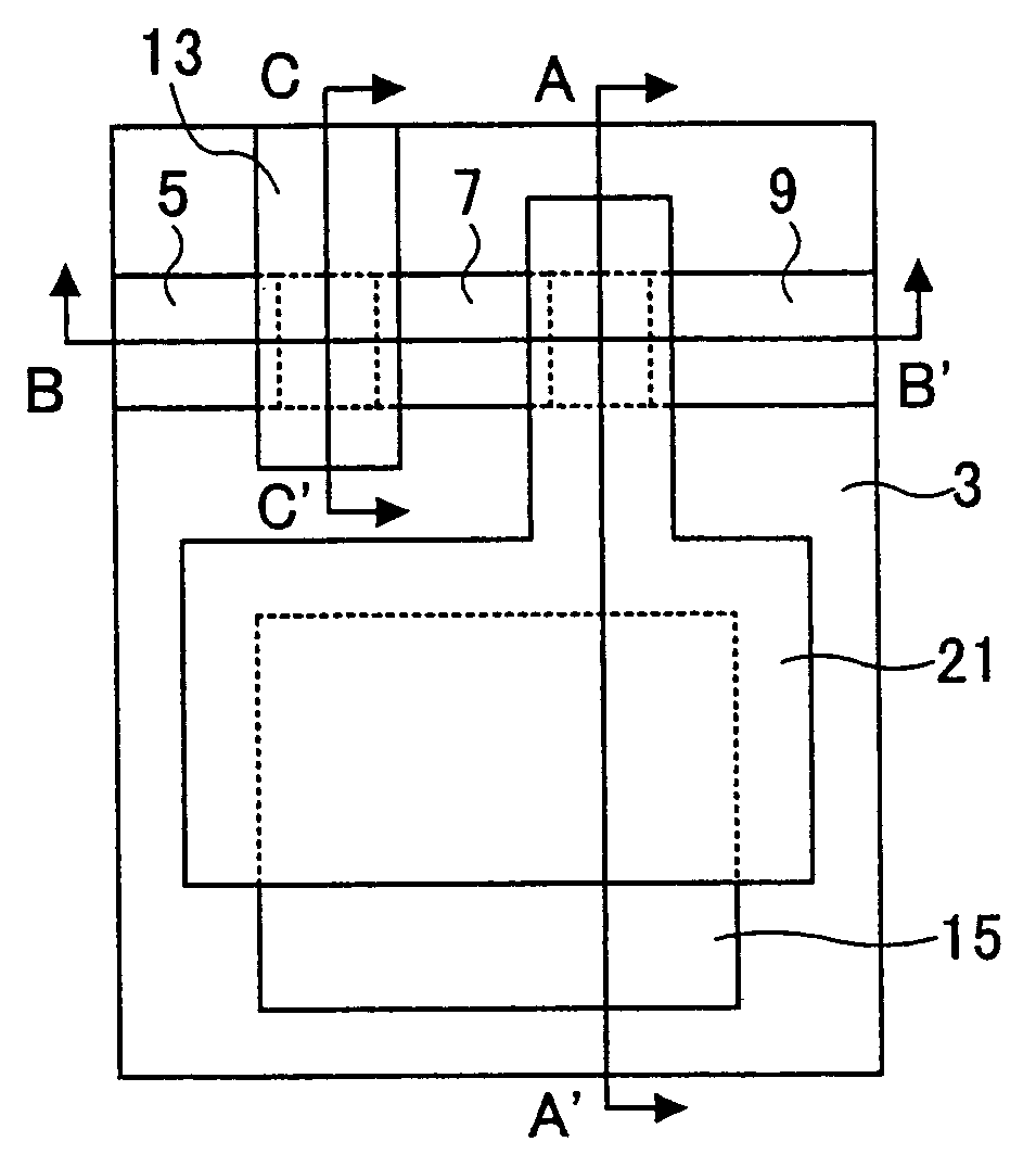
[0086]FIG. 1 shows the semiconductor device. A plan view is shown at sub-section (A), a sectional view in the A-A′ cross-section of the sub-section (A) is shown at sub-section (B), a sectional view in the B-B′ cross-section of the sub-section (A) is shown at sub-section (C), and a sectional view in the C-C′ cross-section of the sub-section (A) is shown at sub-section (D). Although this embodiment describes only one memory unit, the embodiment is applicable to any number of memory units. This embodiment is explained with reference to FIG. 1.

[0087] A field oxide film 3 (first insulation film) for unit separation is formed on the surface of a P substrate 1 in thickness, for example, between 4500 A and 7000 A. Here, in this embodiment, the film is formed 5000 A thick. N type diffusion layers 5, 7, and 9 are formed in an active region of the P substrate 1 surrounded by the field oxide film 3. The N type diffusion layers 5 and 7 are formed with an interval, and the N type diffusion layers...

second embodiment

[0114] The memory unit of the semiconductor device is provided with the laminating film 31 that contains the silicon nitride film through which an electron cannot travel easily between the control gate 15 and the floating gate 21, thereby the reliability of the memory is enhanced.

[0115]FIG. 6 shows sectional views for explaining the second embodiment of the manufacturing method for manufacturing the semiconductor device of the second embodiment, the sectional views being in the A-A′ cross-section and C-C′ cross-section of the sub-section (A) of FIG. 5. Sectional views in the B-B′ cross-section of the sub-section (A) of FIG. 5 is the same as FIG. 4. The embodiment of this manufacturing method is explained with reference to FIG. 4 through FIG. 6.

[0116] (1) The field oxide film 3 for unit separation is formed on the P substrate 1 by the usual LOCOS method. The sacrifice oxide film 23 is formed on the active region surface demarcated by the field oxide film 3, and a channel dope inject...

fifth embodiment

[0156] In the semiconductor device, since the tunnel oxide film 53 with film thickness thinner than the gate oxide film 19 for the memory is formed, writing to and erasing the memory can be performed through the tunnel oxide film 53, and the flexibility in designing the memory characteristic is enhanced.

[0157]FIG. 13 and FIG. 14 show sectional views for explaining the fifth embodiment of the manufacturing method for manufacturing the semiconductor device of the fifth embodiment. FIG. 13 shows the sectional view in the A-A′ cross-section and in the C-C′ cross-section of the sub-section (A) of FIG. 12, and FIG. 14 shows the sectional view in the B-B′ cross-section of the sub-section (A) of FIG. 12. The embodiment of this manufacturing method is explained with reference to FIG. 12 through FIG. 14.

[0158] (1) The field oxide film 3 for unit separation is formed on the P substrate 1 by the usual LOCOS method. A sacrifice oxide film in film thickness between 250 A and 400 A is formed on t...


PUM


Abstract

A semiconductor device is capable of being applied with both a positive and a negative voltage to its control gate, and writing to its memory requires a low voltage. A control gate is formed on a memory unit region of a field oxide film, and an inter-layer silicon oxide film is formed on its surface. A gate oxide film for a non-volatile memory is formed on a P substrate between N type diffusion layers. The floating gate is formed on the inter-layer silicon oxide film, the field oxide film, and the gate oxide film for the non-volatile memory. Since a large coupling ratio between the control gate and the floating gate is available on the field oxide film, memory rewriting requires only a low voltage. Further, since the control gate is formed by a poly silicon film, both a positive voltage and a negative voltage can be applied to the control gate.

Description

TECHNICAL FIELD [0001] The present invention generally relates to a semiconductor device and a manufacturing method thereof, and especially relates to a semiconductor device equipped with a non-volatile memory, and manufacturing method thereof. [0002] In this specification, a first electric conduction type is a P type or an N type, and a second electric conduction type is an N type or a P type, an electric conduction type reverse to the first electric conduction type, respectively. BACKGROUND ART [0003] As kinds of a non-volatile memory called EEPROM (electrically erasable programmable random memory), there are generally two kinds that are differentiated by quantities of gates. Namely, they are a one-layer gate type and a two-layer gate type. As for the one-layer gate type, technology has been available, such as presented by Japan Provisional Publications No. 6-85275 and No. 8-506693. As for the two-layer gate type, technology has been available, such as presented by Japanese Patent...

Claims


Application Information

Patent Timeline
Patent Type & Authority Applications(United States)
IPC IPC(8): H01L21/8247H01L27/115H01L29/423H01L29/788H01L29/792
CPCH01L27/115H01L27/11521H01L27/11526H01L27/11534H01L27/11558H01L29/42324H01L29/7883H10B41/43H10B41/40H10B41/60H10B69/00H10B41/30
Inventor IWAI, MORIYAYOSHIDA, MASAAKINAKANISHI, HIROAKI
Owner RICOH KK
Why Eureka
Try Eureka