Method for reducing silicon wafer film thickness difference in furnace tube process

A furnace tube process and film thickness technology, applied in metal material coating process, coating, gaseous chemical plating and other directions, can solve the problem of large difference in thickness of silicon wafers, reduce film thickness difference, improve thickness difference, reduce Effects of concentration differences

Pending Publication Date: 2020-11-03
SHANGHAI HUALI INTEGRATED CIRCUTE MFG CO LTD
View PDF7 Cites 0 Cited by
  • Summary
  • Abstract
  • Description
  • Claims
  • Application Information

AI Technical Summary

Problems solved by technology

[0010] The technical problem to be solved by the present invention is to provide a method for improving the thickness difference of the silicon wafer film in the furnace tube process, which can solve the problem that the thickness difference of the silicon wafer at different positions of the furnace tube is relatively large in the existing process

Method used


Image

  • Method for reducing silicon wafer film thickness difference in furnace tube process
  • Method for reducing silicon wafer film thickness difference in furnace tube process
  • Method for reducing silicon wafer film thickness difference in furnace tube process

Examples


Embodiment 1

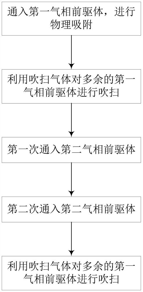
[0029] The method that the embodiment of the present invention provides to improve the difference in thickness of the silicon wafer film in the furnace tube process, such as figure 1 As shown, the growth of the film comprises several cyclic processes, and the steps of each cyclic process are as follows:

[0030] Step S1, introducing the first gas phase precursor for physical adsorption;

[0031] Step S2, using a purge gas to purge the redundant first gas phase precursor;

[0032] Step S3, the second gas-phase precursor is introduced for the first time, and the flow rate of the second gas-phase precursor is S 1 , the access time is T 1 ;

[0033] Step S4, the second gas-phase precursor is introduced for the second time, and the flow rate of the second gas-phase precursor is S 2 , the access time is T 2 ;

[0034] Step S5, using a purge gas to purge the excess second gas-phase precursor;

[0035] Wherein, the volume V of the second gas phase precursor required in each cyc...

Embodiment 2

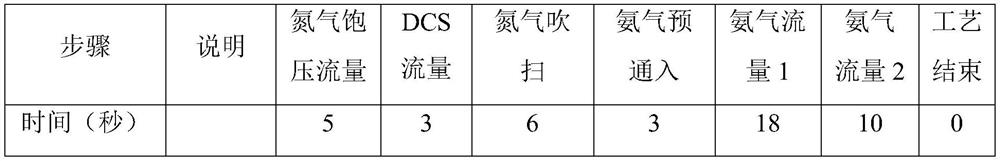
[0044] On the basis of the first embodiment, this embodiment further defines in detail the method for improving the thickness difference of the silicon wafer film in the furnace tube process.

[0045] Wherein, the ratio of the flow rate S1 of the second gas-phase precursor introduced for the first time to the flow rate S2 of the second gas-phase precursor introduced for the second time is 5:1˜10:1.

[0046] In step S2 and step S5, the purge gas is nitrogen or inert gas.

[0047] In step S3 and step S4, the second gas-phase precursor and the first gas-phase precursor perform a chemical reaction to form a thin film.

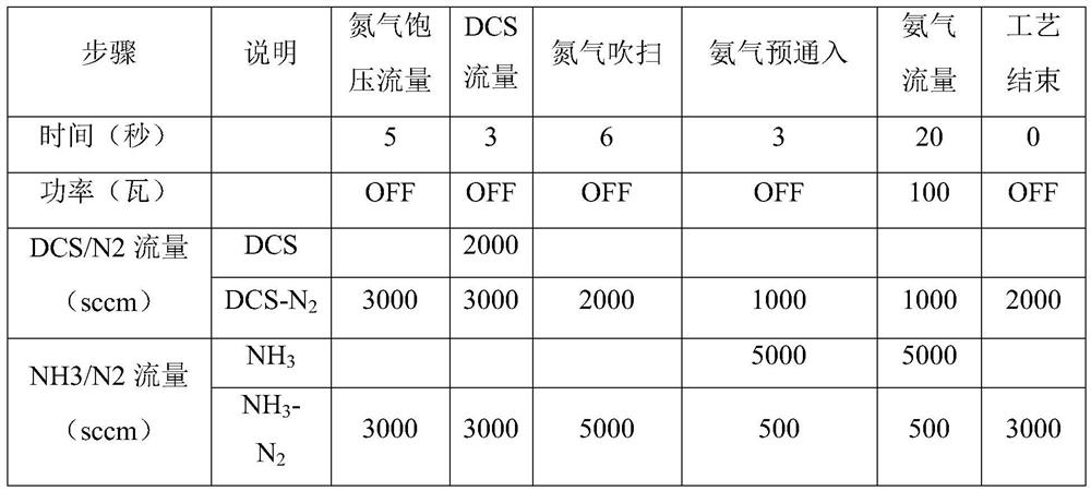
[0048] The silicon nitride thin film formed by atomic layer deposition (ALD) process is taken as an example for illustration below.

[0049] The thickness of the film depends on the specific number of cycles. At present, each cycle of deposition includes: 1) feeding DCS (dichlorodihydrosilane) gas for the first physical adsorption; 2) purging excess DCS gas sourc...


PUM


Abstract

The invention discloses a method for reducing silicon wafer film thickness difference in a furnace tube process. Each circulation process comprises the following steps of S1, introducing a first gas-phase precursor; S2, blowing the redundant first gas-phase precursor; S3, introducing a second gas-phase precursor for the first time; S4, introducing a second gas-phase precursor for the second time;and S5, blowing the redundant second gas-phase precursor; wherein the relationship, among the volume V0 of the second gas-phase precursors required in each circulation process, the flow S1 and the introduction time T1 of the second gas-phase precursor introduced for the first time, and the flow S2 and the introduction time T2 of the second gas-phase precursor introduced for the second time, is V0=S1xT1+S2xT2; and S1>S2. According to the method, on the premise of ensuring that the thickness of a thin film deposited in each circulation process is not changed, the concentration difference of precursor residual gas in a furnace tube is effectively reduced, the film thickness difference, caused by residual gas deposition, of silicon wafers at different positions in the furnace tube is reduced,and the thickness difference among the silicon wafers is improved.

Description

technical field [0001] The invention relates to the technical field of semiconductor manufacturing, in particular to a method for improving the thickness difference of a silicon wafer film in a furnace tube process. Background technique [0002] In the process of growing thin films using the furnace tube process, the control of the film growth steps is all controlled by time without exception. When the set growth time is reached, correspondingly, the input of the reaction gas is stopped, and the flow rate of the relevant reaction gas is also reset to zero from the set value. [0003] For example, silicon nitride (Si 3 N 4 ) film has excellent characteristics such as strong blocking ability to mobile ions (Na+), compact structure, small pinhole density, hydrophobicity, good chemical stability, and large dielectric constant. It is a kind of semiconductor, microelectronics and MEMS. Thin film materials are widely used in the field, and are widely used in passivation, isolati...

Claims


Application Information

Patent Timeline
Patent Type & Authority Applications(China)
IPC IPC(8): C23C16/34C23C16/30C23C16/40C23C16/455
CPCC23C16/345C23C16/308C23C16/45525C23C16/402
Inventor 成鑫华
Owner SHANGHAI HUALI INTEGRATED CIRCUTE MFG CO LTD
Why Eureka
Try Eureka