Device for grinding and cutting wafer

A grinding, wafer technology, applied in the direction of grinding device, grinding/polishing equipment, grinding machine, etc.

Active Publication Date: 2008-02-13
DISCO CORP
View PDF2 Cites 11 Cited by
  • Summary
  • Abstract
  • Description
  • Claims
  • Application Information

AI Technical Summary

Problems solved by technology

However, in the case of a multi-axis grinder that has a plurality of grinding axes for rough grinding and finish grinding, and sequentially performs rough grinding and finish grinding on wafers on a plurality of chuck tables by rotating the turntable, For the grinding device, there is no device with a mechanism capable of adjusting the opposing position of the grinding wheel and the wafer.

Method used


Image

  • Device for grinding and cutting wafer
  • Device for grinding and cutting wafer
  • Device for grinding and cutting wafer

Examples


Embodiment Construction

[0035] Hereinafter, one embodiment of the present invention will be described with reference to the drawings.

[0036] (1) Semiconductor wafer

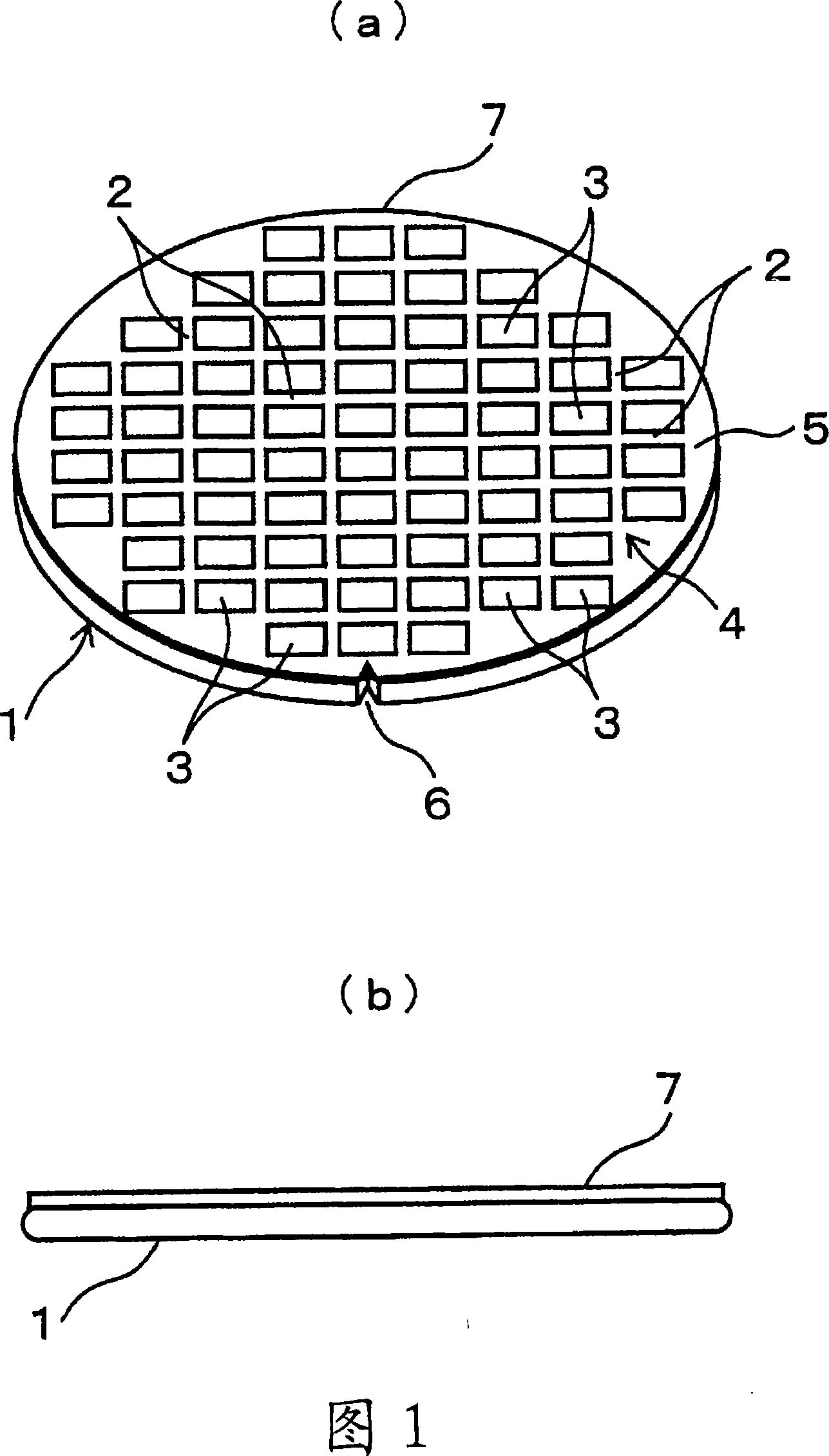
[0037] Reference numeral 1 in FIG. 1 denotes a disk-shaped semiconductor wafer (hereinafter, simply referred to as a wafer) having recesses formed on the back surface thereof by a wafer grinding apparatus according to one embodiment. The wafer 1 is a silicon wafer or the like, and its thickness before processing is, for example, about 600 to 700 μm. On the surface of the wafer 1, a plurality of rectangular semiconductor chips 3 are divided by grid-like dividing lines 2, and IC (Integrated circuit: integrated circuit), LSI (Large Scale Integration: large-scale integration) are formed on the surface of these semiconductor chips 3. circuit) and other electronic circuits not shown in the figure.

[0038] A plurality of semiconductor chips 3 are formed in an approximately circular-shaped device formation region 4 concentric with the wafe...


PUM


Abstract

The present invention provides a wafer grinding device. In a multiaxial grinding device with a plurality of grinding axis, to adjust the position of a grinding wheel replaced according to the size of the wafer so as to make a grinding blade pass through the rotary center of the wafer, the inner edge of the outer peripheral forms a concave position. When a rotary platform (20) rotating, a chuck worktable (30) is located at a coarse grinding position and a thin grinding position, setting a coarse grinding unit (40A) for coarse grinding and a thin grinding unit (40B) for thin grinding to the wafer (1) holding on the chuck worktable (30) at each position. To ensure the grinding units (40A, 40B) move freely along an axis between the rotary center of the chuck worktable (30) and the rotary center of the rotary platform (20), so as to adjust the position of the grinding wheel (45) of each grinding units (40A, 40B) to relative to the concave position formed based on the size of the wafer.

Description

technical field [0001] The present invention relates to a wafer grinding apparatus for grinding the back surface of a wafer such as a semiconductor wafer to reduce the thickness of the wafer to a predetermined thickness, and particularly relates to a device suitable for grinding only a device forming region inside the outer peripheral portion while leaving the outer peripheral portion aside. Wafer grinding device. Background technique [0002] Semiconductor chips of devices used in various electronic devices are generally manufactured by dividing the surface of a disk-shaped semiconductor wafer into grid-shaped rectangular areas with predetermined division lines called streets, The surface of the area forms the electronic circuits, and then the backside is ground to thin the wafer and singulated along the die lanes. In addition, in recent years, the miniaturization and thinning of electronic equipment have been remarkable, and semiconductor chips have also been required to ...

Claims


Application Information

Patent Timeline
Patent Type & Authority Applications(China)
IPC IPC(8): B24B7/22B24B7/04H01L21/304B24B37/10
Inventor 桑名一孝
Owner DISCO CORP
Why Eureka
Try Eureka