Methods of manufacturing semiconductor device

A manufacturing method and semiconductor technology, applied in the fields of semiconductor/solid-state device manufacturing, semiconductor devices, electric solid-state devices, etc., can solve problems such as damaged devices, wafer damage, process loss, etc.

Inactive Publication Date: 2008-02-20
TAIWAN SEMICON MFG CO LTD
View PDF0 Cites 15 Cited by
  • Summary
  • Abstract
  • Description
  • Claims
  • Application Information

AI Technical Summary

Problems solved by technology

The above-mentioned dust particles will damage the devices located in other parts of the wafer, and if they are not effectively removed during the process, the above-mentioned dust particles will damage other non-fragmented devices in the subsequent process in the form of, for example, scratches. Wafers cause damage, resulting in greater process loss

Method used


Image

  • Methods of manufacturing semiconductor device
  • Methods of manufacturing semiconductor device
  • Methods of manufacturing semiconductor device

Examples


Embodiment Construction

[0050] In order to make the above and other objects, features, and advantages of the present invention more comprehensible, the preferred embodiments are listed below, together with the accompanying drawings, and are described in detail as follows:

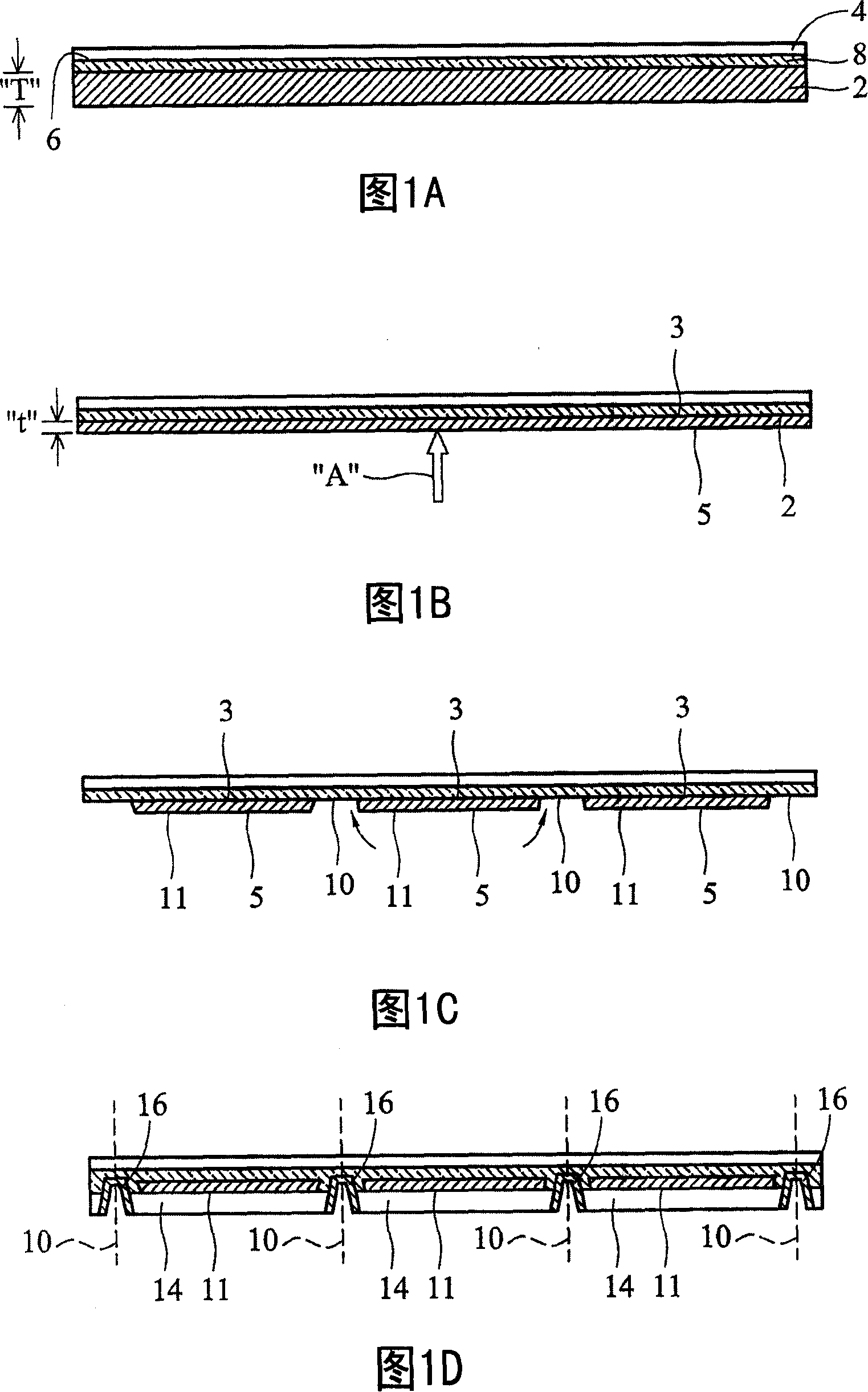
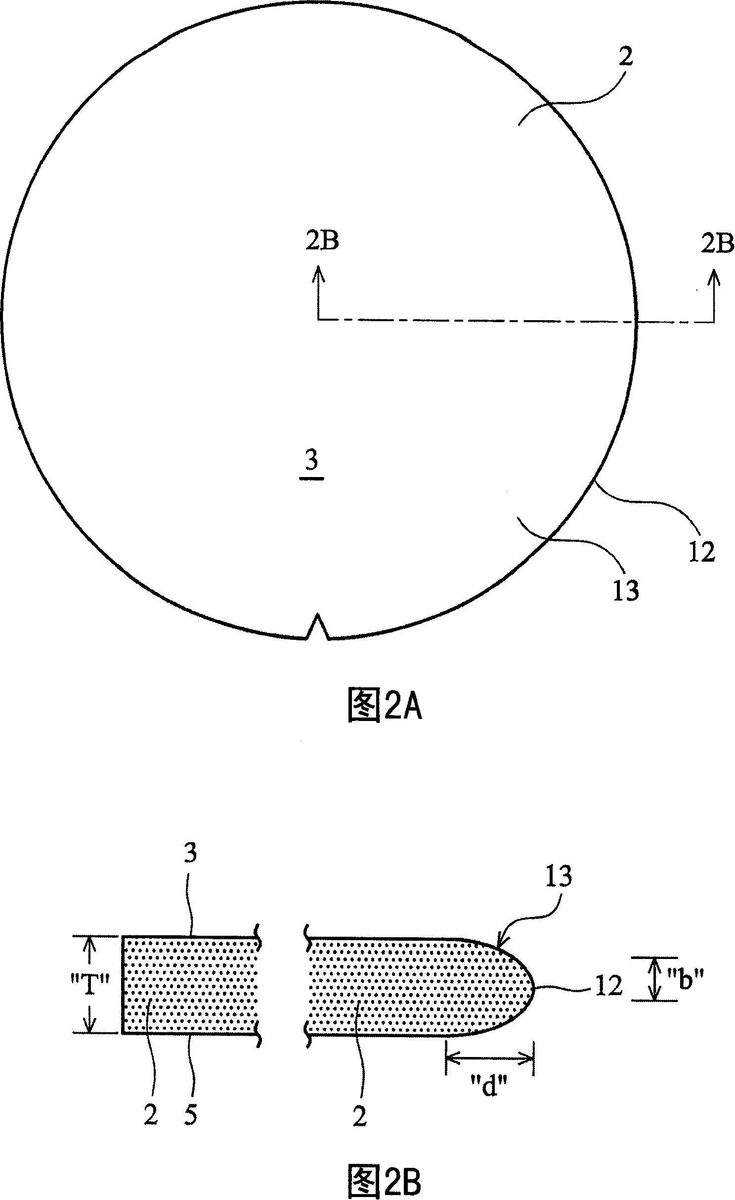
[0051]In an embodiment of the present invention, a process method is disclosed, which can reduce the problem of semiconductor wafer chipping caused by the step of wafer thinning in the process of back photosensitive CMOS device. Specifically, the first embodiment discloses trimming the edge portion of the wafer circumference before the wafer thinning process, and the trimming process can be performed before or after the wafer is connected to a carrier substrate.

[0052] Please refer to FIGS. 1A-1D , which are a series of schematic cross-sectional views showing a series of exemplary process steps for manufacturing a backside photosensitive CMOS image chip. Figure 1A shows a silicon wafer (semiconductor wafer or CMOS wafer) 2 conne...


PUM


Abstract

A process for forming backside illuminated devices is disclosed. Specifically, the process reduces processing damage to wafers caused by poor bond quality at the wafer edge ring. In one embodiment, a wafer edge trimming step is implemented prior to bonding the wafer to the substrate. A pre-grind blade is used to create a straight edge around the wafer perimeter, eliminating any sharp edges. In another embodiment, edge trimming is performed after the wafer has been bonded to the substrate, and a pre-grind blade is used to remove portion of the wafer edge ring subject to poor bonding quality before grinding. The final thickness of the ground wafer is about 50 microns in either case.

Description

technical field [0001] The present invention relates to semiconductor technology, and more particularly to a process for reducing wafer damage by trimming the bevel edge of the wafer before grinding the wafer. Background technique [0002] Existing complementary metal oxide semiconductor (CMOS) or charge coupled device (CCD) image sensors use traditional front-side photosensitive technology to capture images. However, front photosensitive technology has significant limitations in operation, such as low fill factor (the ratio of the area that can absorb light in a single pixel to the entire pixel), low sensitivity (sensitivity), and limited spectral response. (spectral response) and so on, the reason is that the metal circuit structure of the device is formed on the front of the chip in the pixel area, which shields part of the pixel area, thereby reducing the photons reaching the effective area of ​​the pixel. [0003] In order to solve the above problems, especially in app...

Claims


Application Information

Patent Timeline
Patent Type & Authority Applications(China)
IPC IPC(8): H01L21/50H01L21/8238
CPCH01L21/304H01L27/14618H01L27/14687H01L2924/0002H01L2924/00
Inventor 谢元智喻中一萧国裕傅士奇刘铭棋蔡嘉雄
Owner TAIWAN SEMICON MFG CO LTD
Why Eureka
Try Eureka