Apparatus and methods of cleaning substrates

A technology for cleaning equipment and wafers, used in cleaning methods and utensils, cleaning methods using liquids, chemical instruments and methods, etc., and can solve problems such as short circuit of integrated circuits, inconvenience, and general products and methods that do not have suitable structures and methods. , to prevent residual crystallization

Active Publication Date: 2008-02-27
TAIWAN SEMICON MFG CO LTD
View PDF0 Cites 21 Cited by
  • Summary
  • Abstract
  • Description
  • Claims
  • Application Information

AI Technical Summary

Problems solved by technology

The crystallization of the ammonium sulfate residue 180 falling on the wafer 150 may cause a short circuit or an opening in the integrated circuit located on the wafer 150
[0007] This shows that the above-mentioned existing equipment for cleaning substrates and methods thereof obviously still have inconvenience and defects in product structure, method and use, and need to be further improved urgently
In order to solve the above-mentioned problems, the relevant manufacturers have tried their best to find a solution, but no suitable design has been developed for a long time, and there is no suitable structure and method for general products and methods to solve the above-mentioned problems. This is obviously a problem that relevant industry players are eager to solve

Method used


Image

  • Apparatus and methods of cleaning substrates
  • Apparatus and methods of cleaning substrates
  • Apparatus and methods of cleaning substrates

Examples


Embodiment Construction

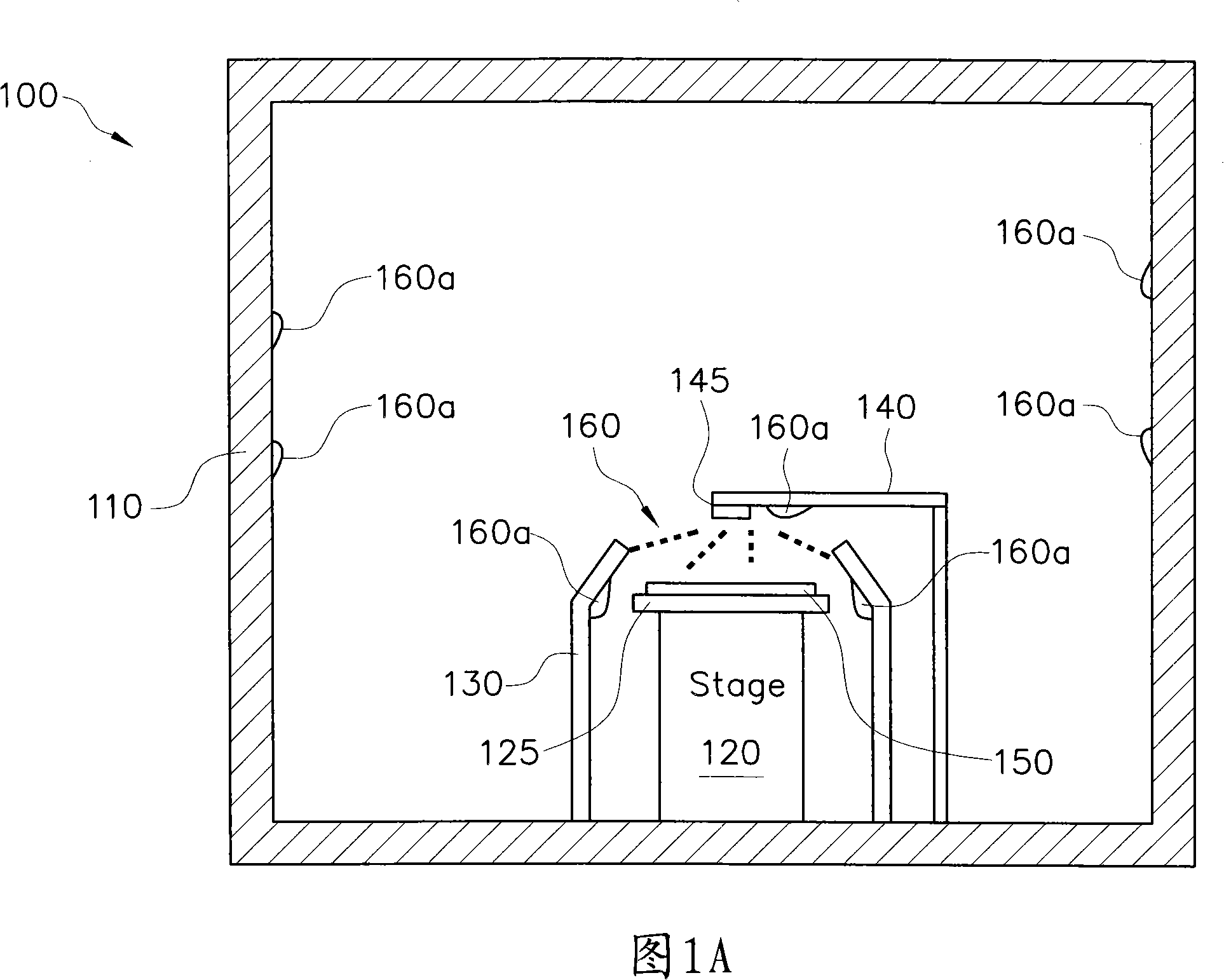
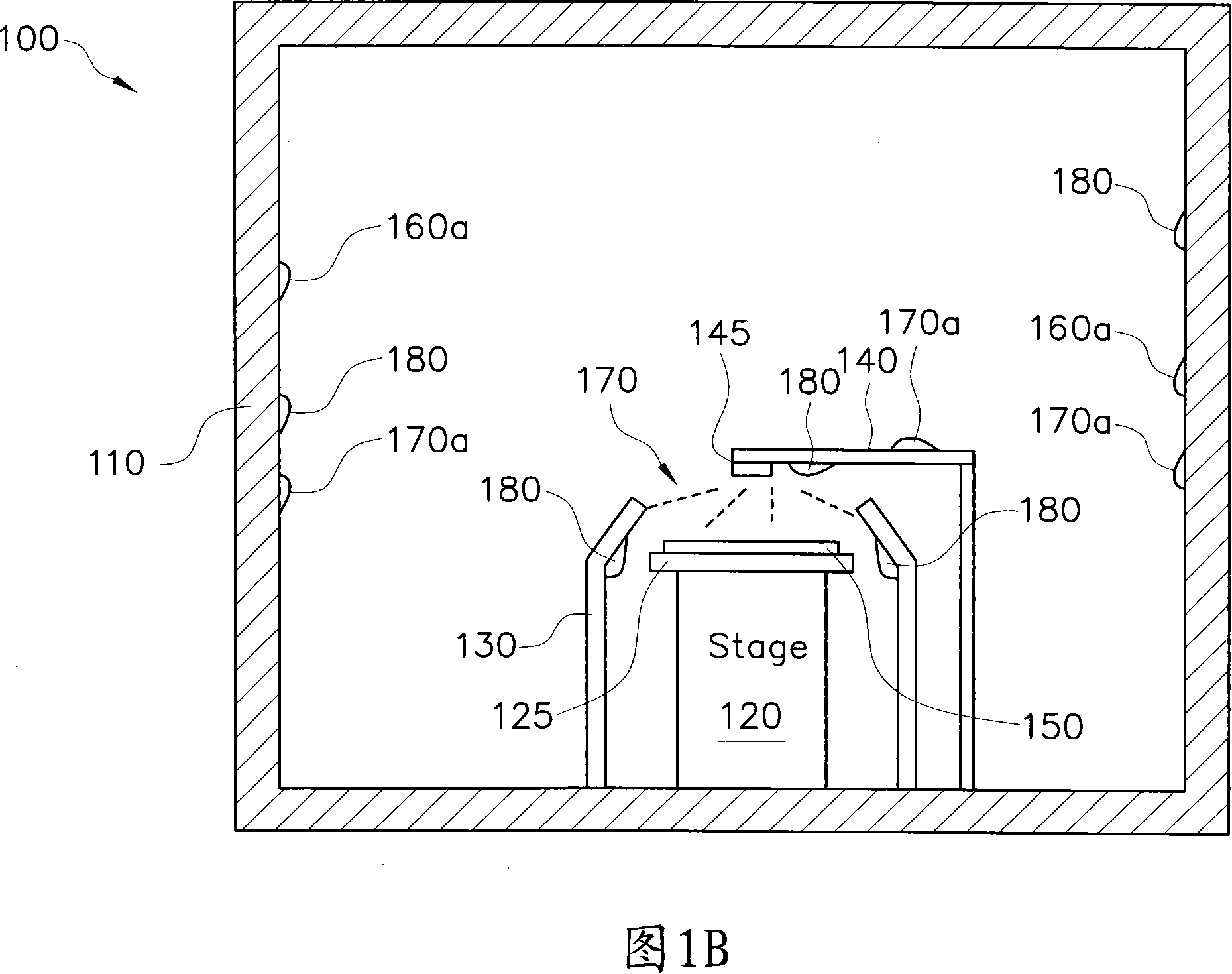
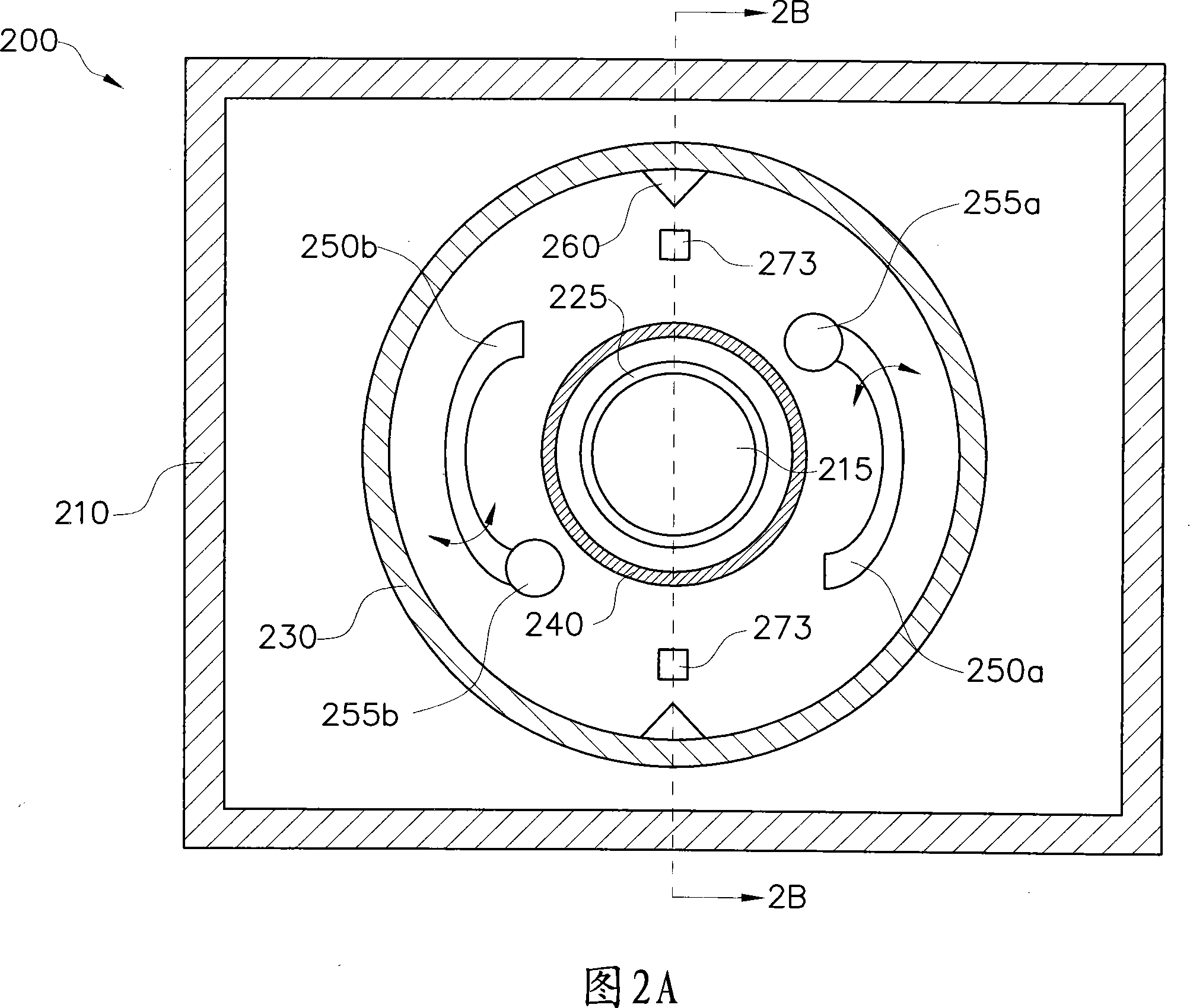
[0066] In order to further explain the technical means and effects of the present invention to achieve the intended purpose of the invention, the specific implementation, structure and method of the wafer cleaning equipment and method proposed according to the present invention will be described below in conjunction with the accompanying drawings and preferred embodiments. , steps, features and effects thereof are described in detail below.

[0067] The embodiments of this description must be read in conjunction with the illustrations, which must be considered part of this description. Relative relative words in the description, such as: higher, lower, parallel, vertical, above, below, up, down, top or bottom, and derivatives of the above words (such as adverbs : Parallel, downward or upward) must refer to the direction shown in the illustration. These relative terms are used only for convenience of description, and are not used to limit the technical features of the present ...


PUM


Abstract

The invention relates to a wafer cleaning method and an apparatus used in said method. The apparatus comprises an enclosure; a stage within the enclosure; at least one first wall around the stage within the enclosure; a plate within the enclosure and above the stage, operable to enclose a first region between the stage and the first wall; and an exhauster part coupled to the first region between the stage and the first wall. The method for cleaning a wafer includes: putting the stage with a wafer into a closed vessel which is arranged in the enclosure; spraying a first chemical onto the surface of a substrate with a first nozzle; spraying a second chemical onto the surface of the substrate with a second nozzle to avoid the products generated by chemical reaction between the first and the second chemical in the first and the second nozzle. The invention is suitable for practicality since an airtight space therein is arranged between a cleaning enclosure and a cleaning stage to avoid short circuit or opening of the integrated circuit on the wafer by means of preventing liquid ammonium sulfate residue from crystallizing when cleaning the wafer.

Description

technical field [0001] The present invention relates to a device for forming a semiconductor structure and a manufacturing method thereof, in particular to a device capable of preventing liquid ammonium sulfate residual crystals in the wafer cleaning process from causing short circuit or generation of integrated circuits located on the wafer. Open wafer cleaning apparatus and method thereof. Background technique [0002] With the development of electronic products, semiconductor technology has been widely used to manufacture memories, central processing units, liquid crystal displays, light-emitting diodes, laser diodes, and components or chipsets. In order to achieve the goal of high integration and high speed, the feature size of semiconductor integrated circuits is still shrinking continuously. At present, many materials and technologies have been developed to achieve the above-mentioned goals of integration and speed, and to overcome the following problems. The ensuing ...

Claims


Application Information

Patent Timeline
Patent Type & Authority Applications(China)
IPC IPC(8): H01L21/306H01L21/67H01L21/00B08B3/08
CPCH01L21/67051B08B2203/0229B08B3/02
Inventor 黄琮民魏正泉江明晁
Owner TAIWAN SEMICON MFG CO LTD
Why Eureka
Try Eureka