Organic semiconductor elements and manufacturing method therefor

A technology of organic semiconductors and manufacturing methods, applied in semiconductor/solid-state device manufacturing, semiconductor devices, electrical components, etc., can solve the problems of SAM volatile quality stability, poor quality, and affecting the characteristics of semiconductor materials, so as to improve the carrier The effect of movement speed

Inactive Publication Date: 2008-03-05
IND TECH RES INST
View PDF0 Cites 3 Cited by
  • Summary
  • Abstract
  • Description
  • Claims
  • Application Information

AI Technical Summary

Problems solved by technology

Therefore, some research is to form a single layer of self-aligned material (SAM) on the metal surface or to modify the semiconductor material to help the semiconductor molecules to arrange, but the single-layer SAM is easy to volatilize and has poor quality stability. ; and the modification of the semiconductor layer will affect the characteristics of the semiconductor material itself

Method used


Image

  • Organic semiconductor elements and manufacturing method therefor
  • Organic semiconductor elements and manufacturing method therefor
  • Organic semiconductor elements and manufacturing method therefor

Examples


Embodiment Construction

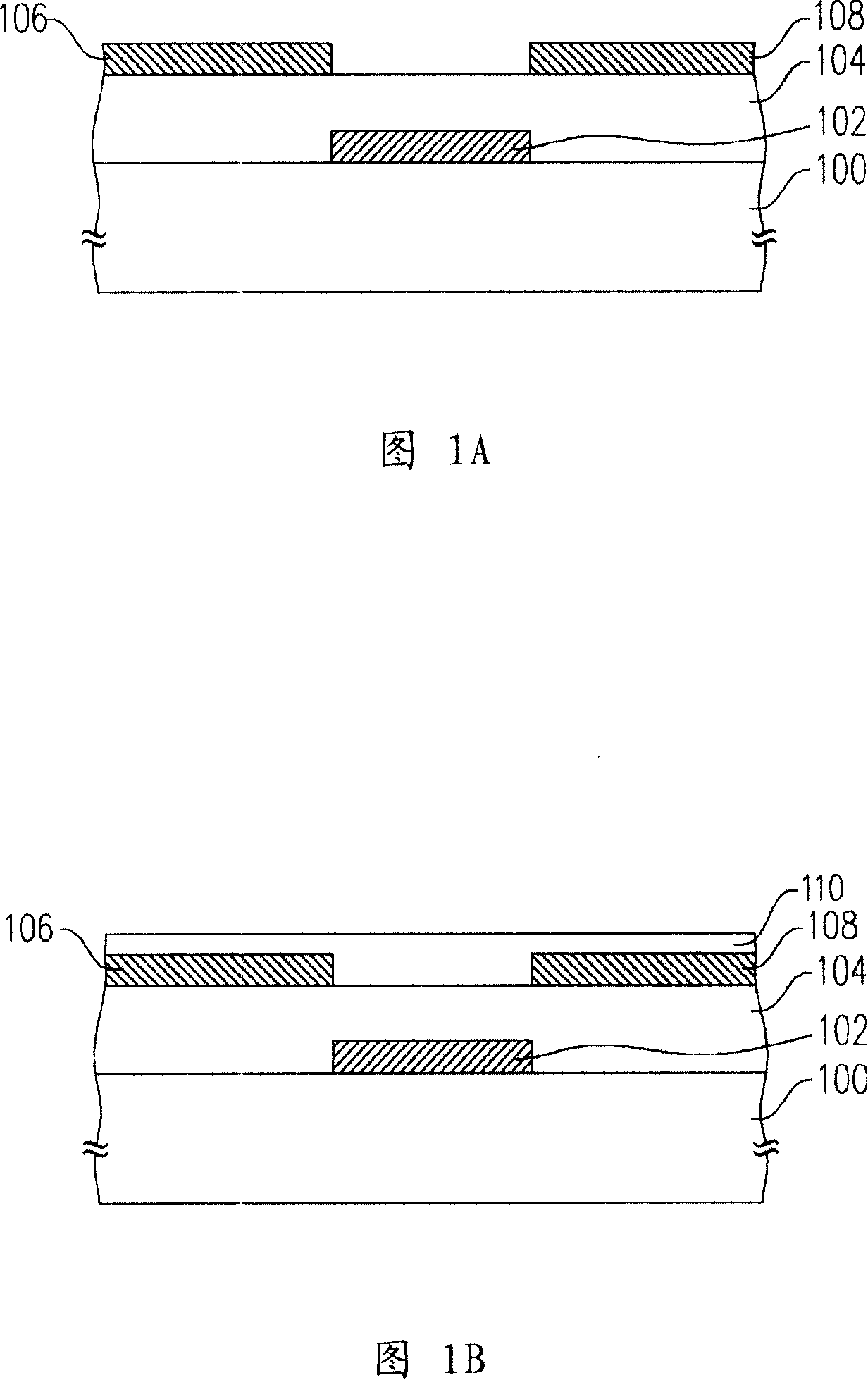
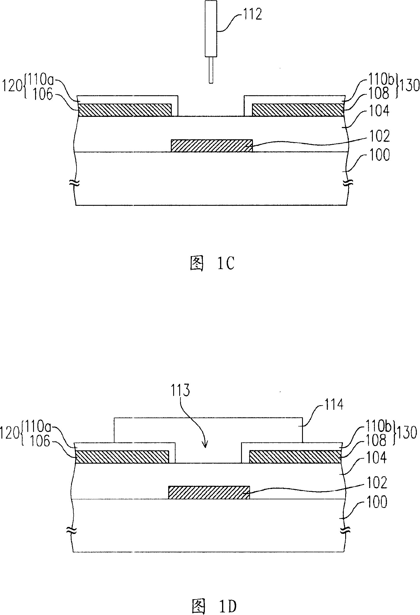
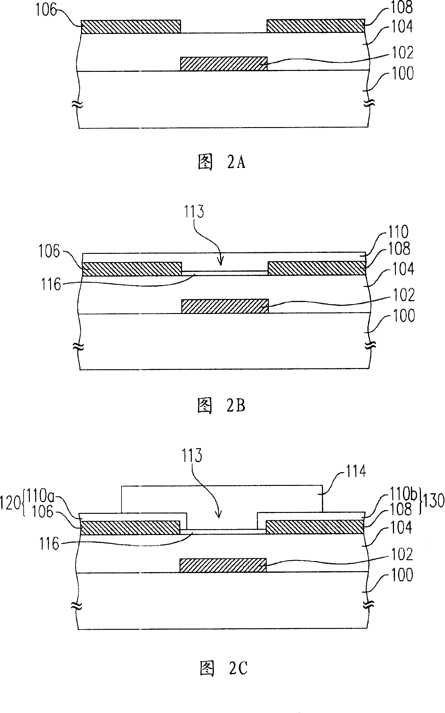
[0036] In the present invention, an organic conductive layer is added between the metal electrode and the organic semiconductor layer, which matches the work function of the semiconductor material, facilitates the arrangement of the organic semiconductor molecules and enables the organic semiconductor molecules in the active layer to be placed on the metal electrode. The crystal grains become larger, so the carrier movement rate of the device can be increased. The present invention can be applied to organic semiconductor elements, which are illustrated by the following examples.

[0037] FIG. 1A to FIG. 1D are cross-sectional views illustrating a process of a method for manufacturing an organic semiconductor device according to an embodiment of the present invention.

[0038] Referring to FIG. 1A , a gate conductor layer 102 is formed on a substrate 100 . The substrate 100 can be a flexible substrate or a rigid substrate, the flexible substrate is made of plastic, and the rig...


PUM


Abstract

This invention relates to a manufacturing method for semiconductor elements, which forms a grid conduction layer and grid dielectric layers on a base orderly, then forms patternized metal layers on the grid dielectric layers at both sides of the conduction layer and forms electrode reformed layer on the top of the metal layers and adjacent side walls to constitute a source and a drain with the covered patternized metal layers and then forms an organic semiconductor layer as an active layer between the source and the drain and above them.

Description

technical field [0001] The present invention relates to an integrated circuit and its manufacturing method, and in particular to an organic semiconductor element and its manufacturing method. Background technique [0002] Organic thin film transistors are transistors made of organic conjugated polymer or oligomolecular materials. Compared with traditional inorganic transistors, organic thin film transistors can be fabricated at low temperatures, so lighter, thinner and cheaper substrates can be used in the selection of substrates. Plastic replaces glass. In addition, organic thin film transistors are relatively simple in manufacturing process, so they have great potential for development. [0003] Although organic thin film transistors have the above-mentioned advantages, there are still some bottlenecks to be overcome in current research, such as slow carrier mobility and high driving voltage. The carrier movement rate is too slow, mainly because the crystal particle size...

Claims


Application Information

Patent Timeline
Patent Type & Authority Applications(China)
IPC IPC(8): H01L51/40H01L51/05
Inventor 黄良莹林宗贤郑翔远胡堂祥
Owner IND TECH RES INST
Why Eureka
Try Eureka