Manufacture of lateral semiconductor devices

A lateral semiconductor, semiconductor technology, applied in semiconductor/solid-state device manufacturing, semiconductor devices, electrical components, etc., can solve the problems of complex manufacturing and increasing the total on-resistance of the device

Inactive Publication Date: 2008-03-05
NXP BV
View PDF4 Cites 6 Cited by
  • Summary
  • Abstract
  • Description
  • Claims
  • Application Information

AI Technical Summary

Problems solved by technology

In contrast, in vertical devices, the drain region is typically formed at the bottom of the structure, and a separate perimeter contact region must be provided extending fro...

Method used


Image

  • Manufacture of lateral semiconductor devices
  • Manufacture of lateral semiconductor devices
  • Manufacture of lateral semiconductor devices

Examples


Embodiment Construction

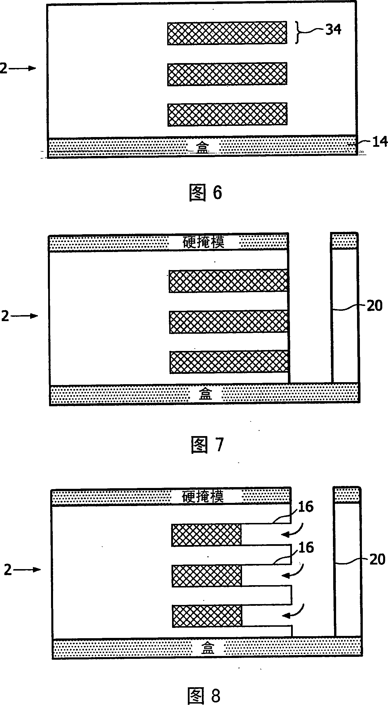
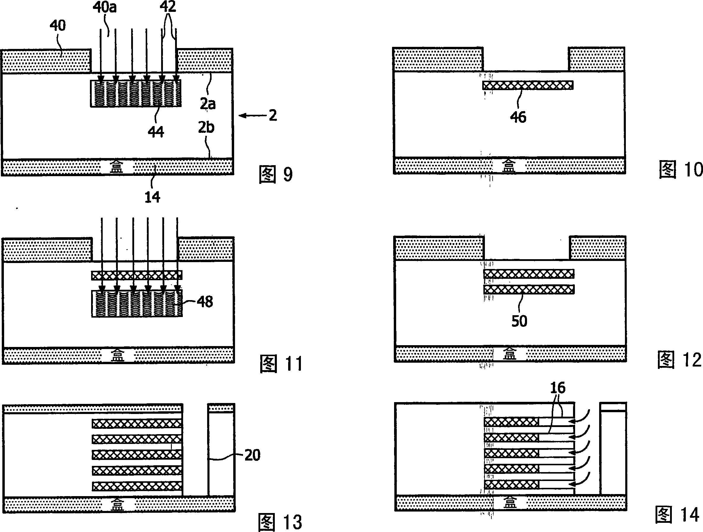
[0063] It should be noted that the diagrams are only diagrams and not drawn to scale. The relative sizes and proportions of the components of these figures have been enlarged and reduced in size, in order to express more clearly and conveniently in the figures. In modified or different embodiments, the same reference symbols are generally used to indicate corresponding or similar features.

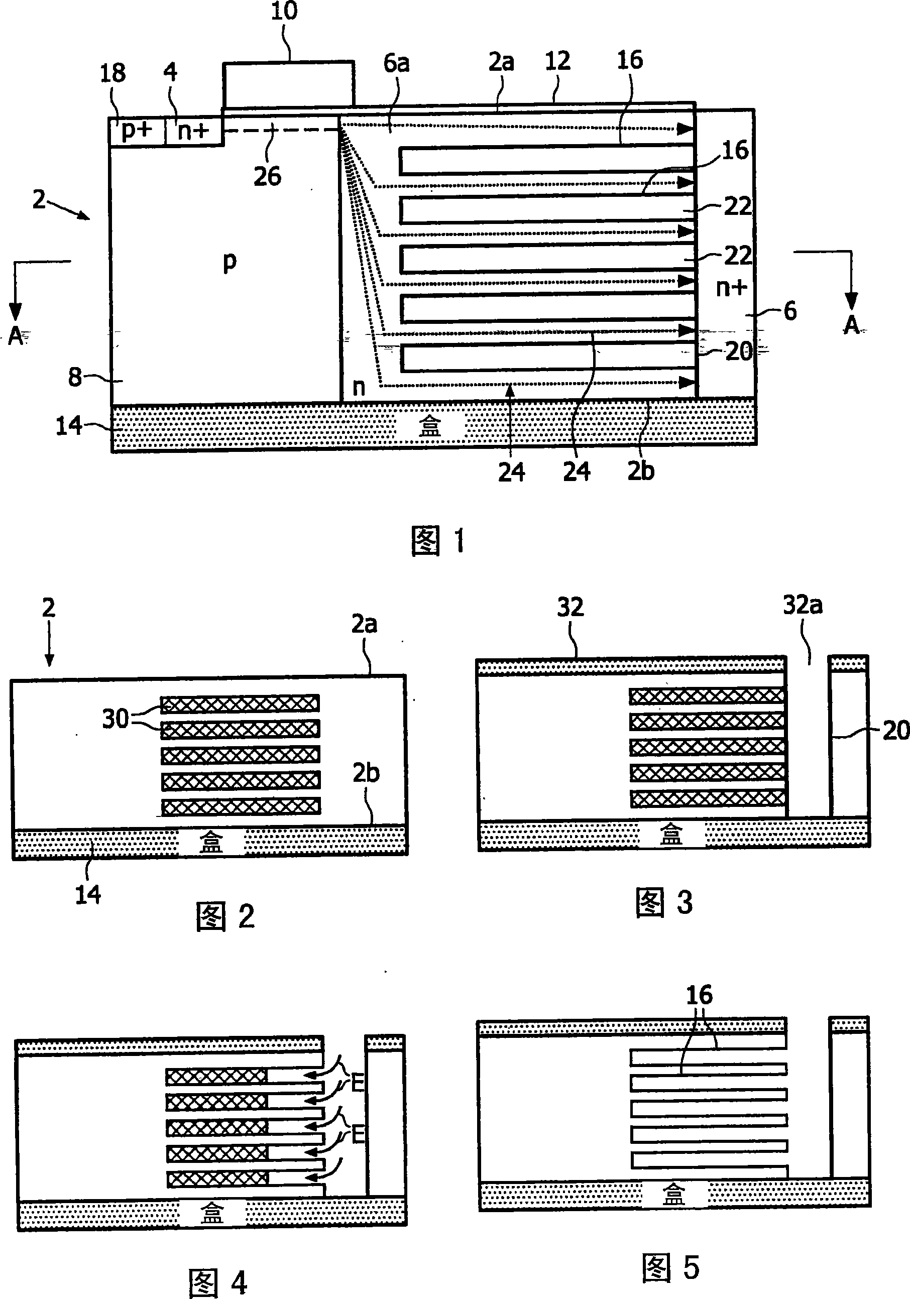
[0064] Fig. 1 shows a cross-sectional side view of a device manufactured by a method according to an embodiment of the present invention. Specifically, the effective area of ​​the device is displayed. The effective area can be bonded around its periphery by various well-known peripheral terminal configurations (not shown).

[0065] The device includes a source region 4 and a drain region laterally spaced apart therefrom. The drain region is composed of a drain drift region 6a that traverses the drain contact region 6 with a higher degree of doping. These regions form part of the semiconductor ...


PUM


Abstract

A method of manufacturing a lateral semiconductor device comprising a semiconductor body (2) having top and bottom major surfaces (2a, 2b), the body including a drain drift region (6a) of a first conductivity type. The method includes the steps of forming a vertical access trench (20) in the semiconductor body which extends from its top major surface (2a) and has a bottom and sidewalls; forming at least one horizontal trench (16) extending within the drain drift region (6a) which extends from a sidewall of the vertical trench (20) in the finished device; and forming a RESURF inducing structure (22) extending within the at least one horizontal trench. In this way, vertically separated lateral RESURF inducing structures are formed without encountering problems associated with known techniques for forming RESURF structures.

Description

Technical field [0001] The present invention relates to methods of manufacturing lateral semiconductor devices, such as insulated gate field effect power transistors (commonly referred to as "MOSFETs"). The present invention also relates to a semiconductor device manufactured by this method. Background technique [0002] Lateral semiconductor devices are mainly used in integrated circuits and not in vertical devices, because the connection to the drain region of the lateral device can be made directly at the top surface of the semiconductor body. In contrast, in a vertical device, the drain region is typically formed at the bottom of the structure, and a separate peripheral contact region extending from the surface to the depth of the buried drain region must be provided, thereby substantially increasing the overall conduction of the device Resistance and complicate the manufacture of the device. [0003] The breakdown voltage of a simple p-n junction depends on the doping level ...

Claims


Application Information

Patent Timeline
IPC IPC(8): H01L21/336H01L29/78H01L29/06H01L29/40H01L29/08H01L21/306H01L21/3065H01L21/265H01L29/423H01L29/417
CPCH01L21/3083H01L29/7824H01L29/7816H01L21/30604H01L29/4175H01L29/0653H01L29/66681H01L29/0847H01L29/7825H01L29/0649H01L21/26506H01L21/3065H01L29/407H01L29/0634H01L21/3247
Inventor 简·雄斯基
Owner NXP BV
Why Eureka
Try Eureka