Substrate bonding apparatus having alignment unit and method of aligning substrates using the same

A technology for substrates and surface plates, which is applied in the field of devices for bonding substrates, can solve problems such as alignment errors, and achieve the effects of increasing productivity and improving alignment efficiency.

Inactive Publication Date: 2008-03-19
ADVANCED DISPLAY PROCESS ENG CO LTD
View PDF0 Cites 26 Cited by
  • Summary
  • Abstract
  • Description
  • Claims
  • Application Information

AI Technical Summary

Problems solved by technology

[0004] At the same time, if the alignment between the two surface plates is not strictly maintained, alignment errors can occur during the alignment operation for substrate bonding

Method used


Image

  • Substrate bonding apparatus having alignment unit and method of aligning substrates using the same
  • Substrate bonding apparatus having alignment unit and method of aligning substrates using the same
  • Substrate bonding apparatus having alignment unit and method of aligning substrates using the same

Examples


no. 1 example

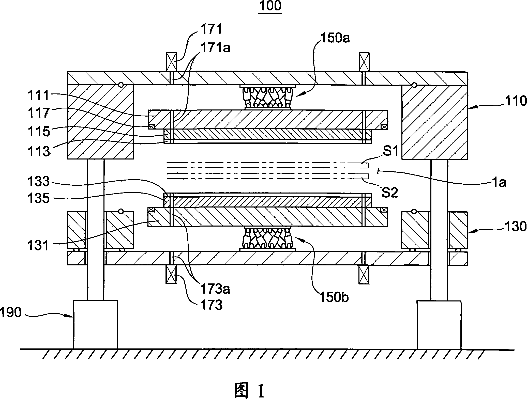
[0026] FIG. 1 is a cross-sectional view schematically showing a substrate bonding apparatus according to a first embodiment of the present invention, wherein the apparatus is indicated generally at 100 . Referring to FIG. 1 , the substrate bonding apparatus includes a first cavity 110 , a second cavity 130 , and an alignment unit 150 . Between the first chamber 110 and the second chamber 130 is formed a processing space 1 a in which the first substrate S1 and the second substrate S2 are bonded to each other. The first and second substrates S1 and S2 may be TFT substrates or color filter substrates.

[0027] The first chamber 110 is provided with a first surface plate 111 on which the first substrate S1 is placed. The first surface plate 111 is provided with a first chuck 113 for connecting the first substrate S1. A first chuck plate 115 for combining the first chuck 113 with the first surface plate 111 is installed between the first surface plate 111 and the first chuck 113 ...

no. 2 example

[0060] FIG. 4 is a cross-sectional view schematically showing a substrate bonding apparatus, indicated generally at 200 , according to a second embodiment of the present invention. Referring to FIG. 4 , the substrate bonding apparatus 200 includes a first chamber 210 and a second chamber 230 provided with a plurality of first surface plates 211 and a plurality of second surface plates 231 , respectively. Therefore, a plurality of first surface plate aligning units 250a are disposed between the first cavity 210 and the respective surface plates 211, and a plurality of second surface plate aligning units 250b are disposed between the second cavity 230 and the respective surface plates 231. . Furthermore, each individual first surface plate 211 (or each individual second surface plate 231 ) is provided with a plurality of distance sensors 217 .

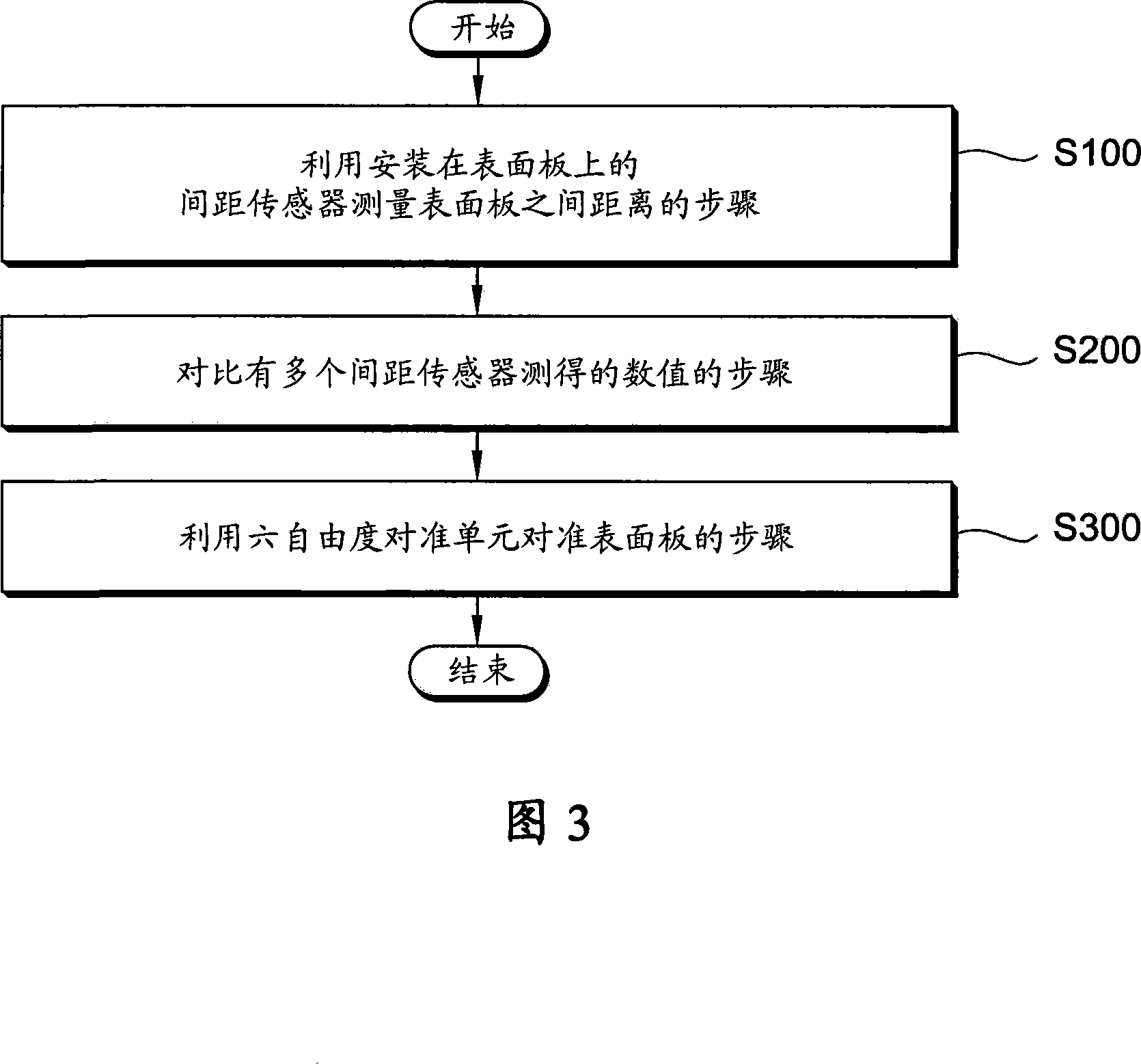
[0061] A plurality of distance sensors 217 installed on the first surface board 211 (or the second surface board 231 ) measures and co...

no. 3 example

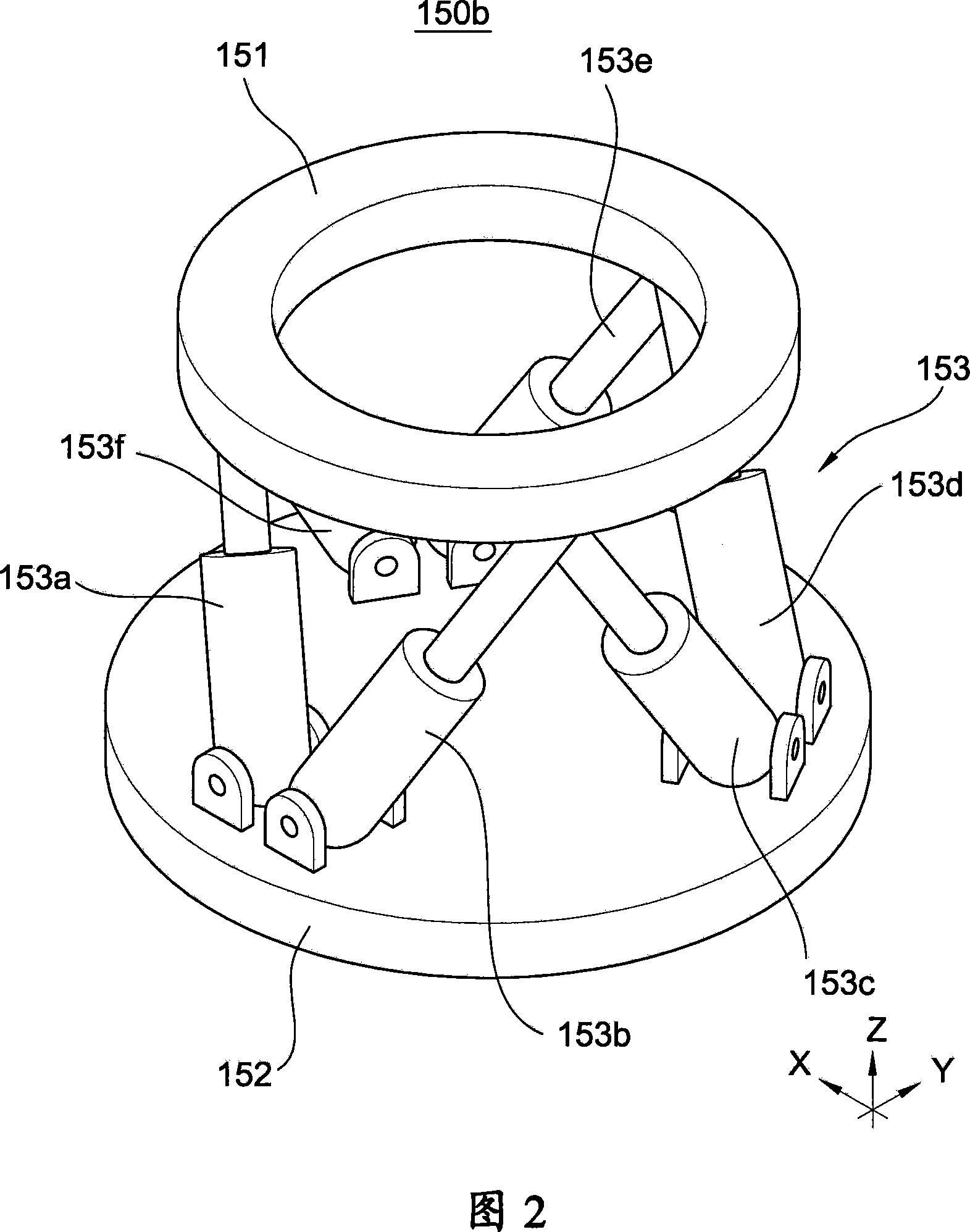
[0063] FIG. 5 is a cross-sectional view schematically showing a substrate bonding apparatus according to a third embodiment of the present invention, wherein the apparatus is generally indicated by reference numeral 300 . Referring to FIG. 5 , the alignment unit 350 is disposed under the second cavity 330 placed under the first cavity 310 . The alignment unit 350 is installed to support the second chamber 330 in such a manner that the connection plate 351 of the alignment unit 350 is attached to the bottom of the second chamber 330 and the support plate 352 is attached to the bottom plate on which the substrate bonding device 300 is mounted.

[0064] A plurality of distance sensors 317 installed on the first surface board 311 (or the second surface board 331 ) measures and compares the distance values ​​between the first and second surface boards. According to the measurement and comparison results, the alignment unit 350 performs six degrees of freedom alignment with respect ...


PUM


Abstract

A substrate bonding apparatus includes a first chamber having a first surface plate where a first substrate is placed. A second chamber is disposed opposite to the first chamber. The second chamber has a second surface plate where a second substrate is placed. The second substrate is to be bonded to the first substrate. An alignment unit is installed in at least one of the first and second chambers. The alignment unit is capable of carrying out a six-degrees-of-freedom alignment between the first and second substrates. Thus, the substrates can be maintained parallel to each other, a spacing between the substrates can be automatically adjusted, and the substrates can be aligned in the X and Y axis directions.

Description

technical field [0001] The present invention relates to an apparatus for bonding substrates, and more particularly, to a substrate bonding apparatus having an alignment unit capable of implementing six degrees of freedom alignment. Background technique [0002] The substrate bonding device is used to bond two substrates of the thin film display device to each other. Examples of thin film display devices include TFT-LCD panels, PDPs, OLEDs, and the like. These thin film display devices are produced in such a manner that a TFT substrate and a color filter substrate are bonded so that they face each other with a gap of several micrometers therebetween. The TFT substrate is provided with a plurality of TFTs (Thin Film Transistors) formed in a matrix, and the color filter substrate is formed of color filters, light-shielding films, and the like. [0003] Substrate bonding is accomplished by pressing the two substrates. Accordingly, the substrate bonding apparatus includes a f...

Claims


Application Information

Patent Timeline
Patent Type & Authority Applications(China)
IPC IPC(8): G02F1/1333H01L21/00H01L21/68
CPCB32B37/0046B32B2457/20H01J9/241G02F2001/133354B30B15/068B30B1/34B32B38/1841G02F1/133354Y10T156/10H01L21/68
Inventor 朴时玄
Owner ADVANCED DISPLAY PROCESS ENG CO LTD
Why Eureka
Try Eureka