Supercharge Your Innovation With Domain-Expert AI Agents!

Semiconductor device

A semiconductor and device technology, applied in the field of semiconductor devices

Inactive Publication Date: 2008-03-19
RENESAS ELECTRONICS CORP
View PDF3 Cites 0 Cited by
  • Summary
  • Abstract
  • Description
  • Claims
  • Application Information

AI Technical Summary

Problems solved by technology

Therefore, a short circuit is easily generated between the gate electrode 312 and the source electrode 317

Method used


Image

  • Semiconductor device
  • Semiconductor device
  • Semiconductor device

Examples


Embodiment Construction

[0028] The invention will now be described herein with reference to illustrative embodiments. Those skilled in the art will recognize that many alternative embodiments can be accomplished using the teachings of the present invention and that the invention is not limited to the illustrative embodiments shown for explanatory purposed.

[0029] Hereinafter, preferred embodiments of the semiconductor device according to the present invention will be explained in detail with reference to the accompanying drawings. Here, when explaining the drawings, the same components are shown with the same reference numerals in all the drawings, and the same explanation will not be repeated.

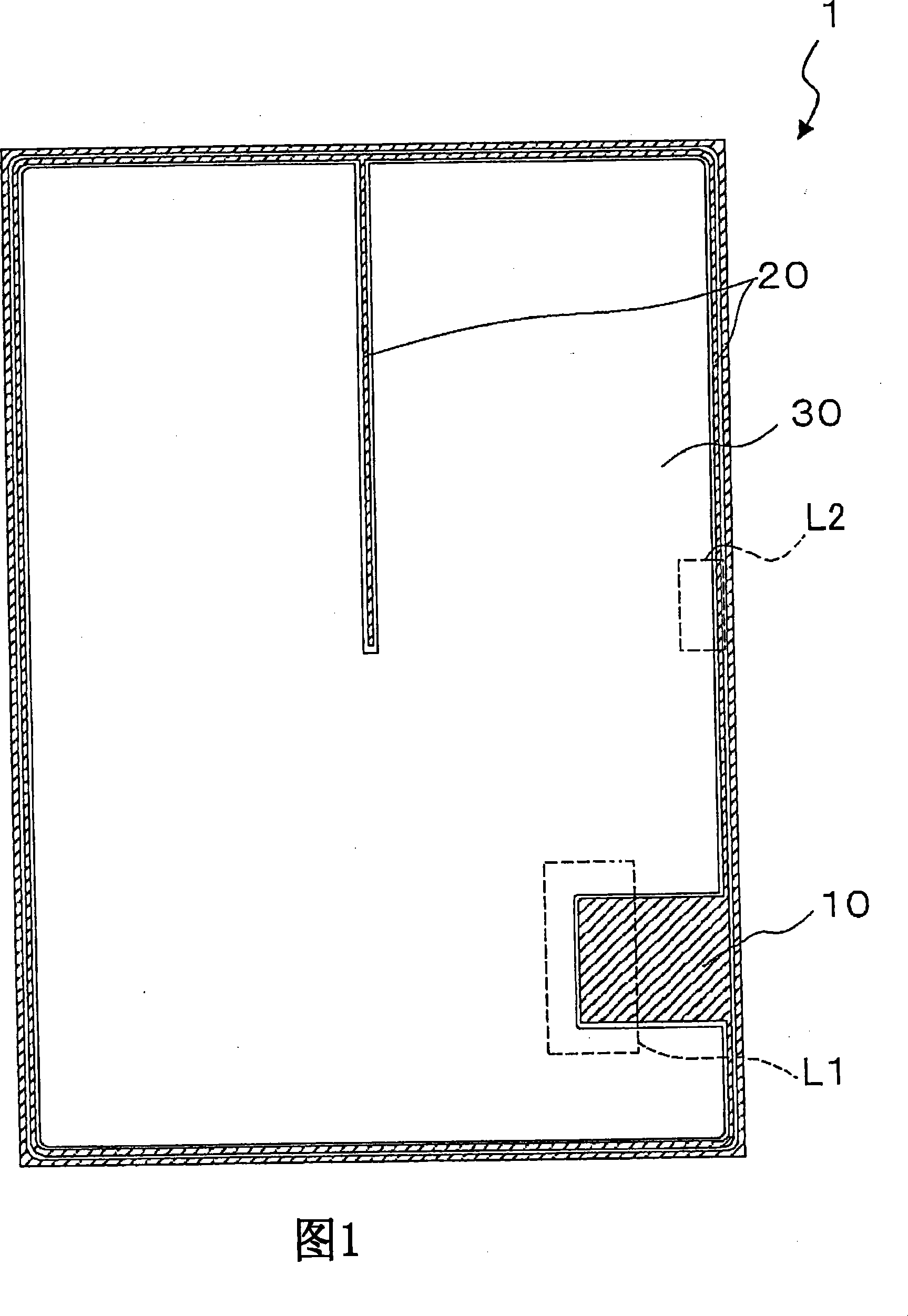
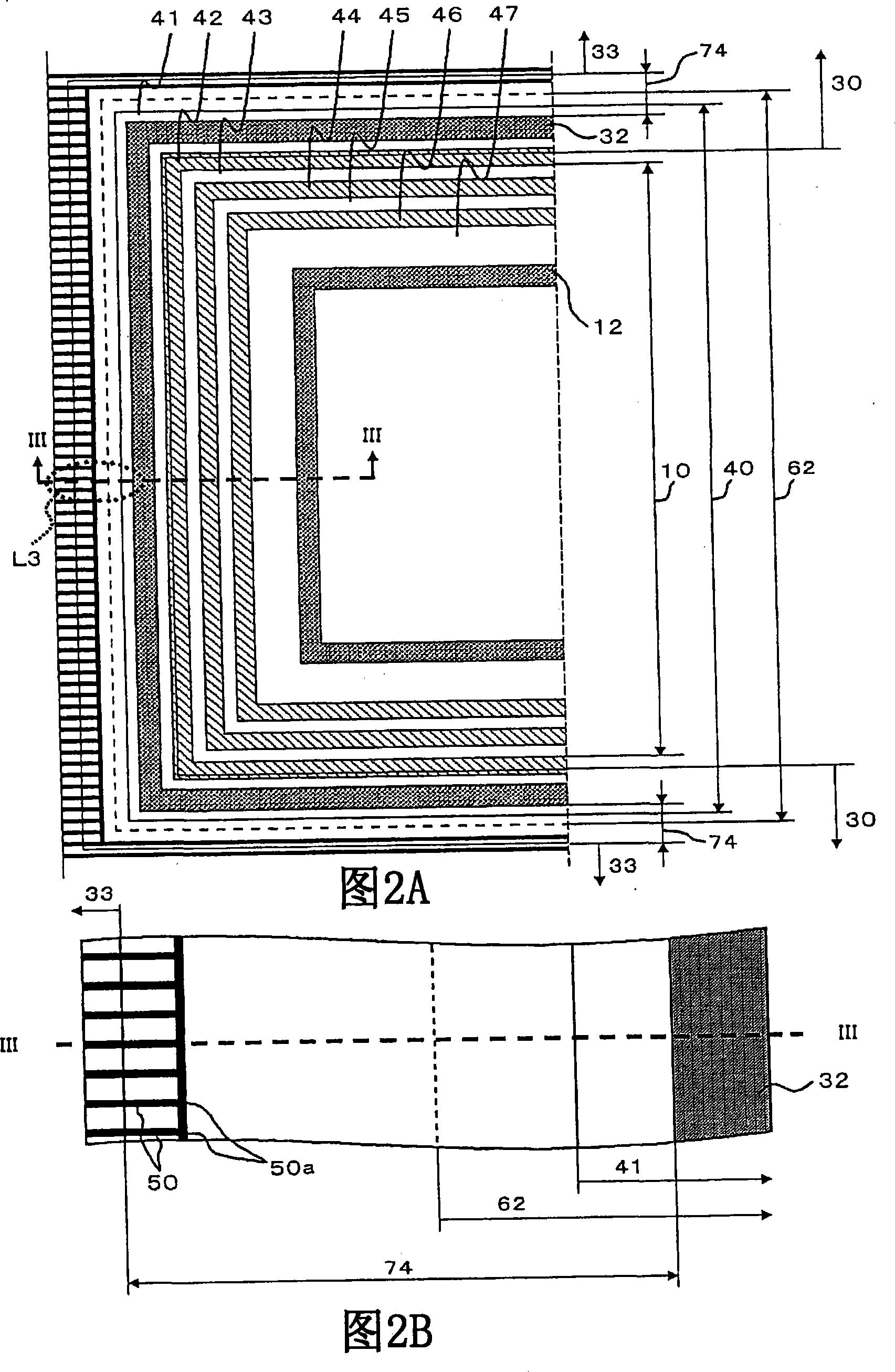
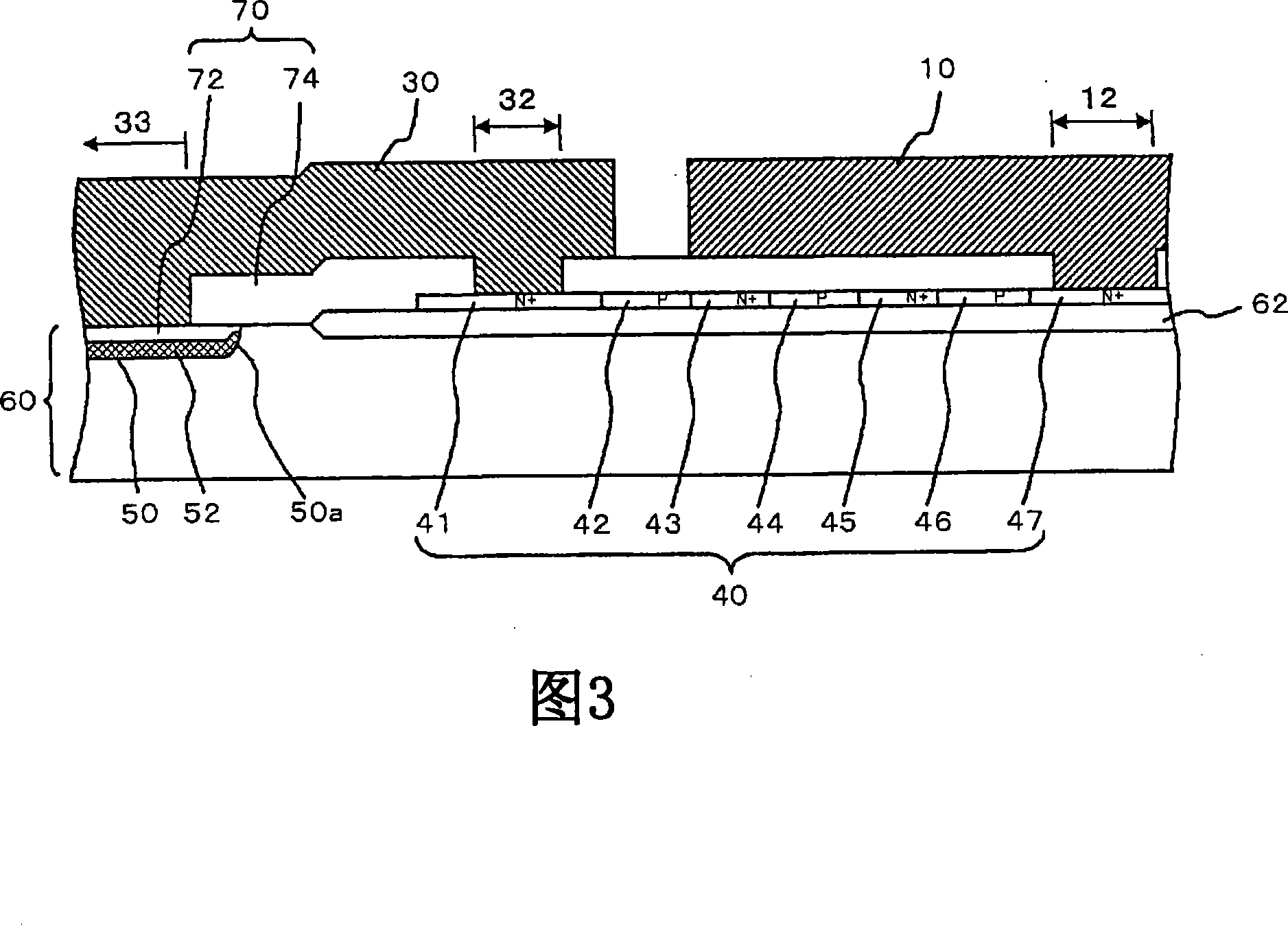
[0030] FIG. 1 is a plan view showing one embodiment of a semiconductor device according to the present invention. The semiconductor device 1 includes: a gate pad 10 ; a gate finger 20 ; and a source electrode 30 . Materials for the gate pad 10 and the source electrode 30 may include, for example, aluminu...


PUM


Abstract

An improved semiconductor device having a gate electrode buried in a trench that a short circuit is hardly generated between a gate electrode and a source electrode at a termination of the gate electrode. A trench is formed in a semiconductor substrate. A gate electrode and a buried insulating film are buried in the trench. A source electrode is provided above the gate electrode via the buried insulating film. At the termination of the gate electrode, an interlayer insulating film is provided between the buried insulating film and the source electrode in such a way that the interlayer insulating film strides over the termination of the trench. Both of the buried insulating film and the interlayer insulating film function as an insulating film and prevent a short circuit at the termination of the gate electrode.

Description

[0001] This application is based on Japanese Patent Application No. 2006-249813, the contents of which are incorporated herein by reference. technical field [0002] The present invention relates to a semiconductor device. Background technique [0003] For example, Japanese Laid-Open Patent Application Publication No. 2000-252468 and Japanese Laid-Open Patent Application Publication No. 2006-60184 have disclosed a conventional semiconductor device having a trench gate structure. In the above semiconductor device, the gate electrode and the insulating film covering the gate electrode are buried in the trench. [0004] 9 is a cross-sectional view showing a semiconductor device described in Japanese Laid-Open Patent Application Publication No. 2000-252468. In the semiconductor device 100 , an N-type drain region 102 and a P-type well region 103 are sequentially stacked on an N+ type semiconductor body 101 . Both the silicon body 101 and the drain region 102 operate as the dra...

Claims


Application Information

Patent Timeline
Patent Type & Authority Applications(China)
IPC IPC(8): H01L29/78H01L29/41
CPCH01L29/7813H01L29/7808H01L29/41741H01L29/42376H01L29/0696H01L27/0629H01L29/7811H01L29/4238
Inventor 山本英雄小林研也
Owner RENESAS ELECTRONICS CORP
Features
  • R&D
  • Intellectual Property
  • Life Sciences
  • Materials
  • Tech Scout
  • Unparalleled Data Quality
  • Higher Quality Content
  • 60% Fewer Hallucinations
Learn More