
Method for model building based on changes of integrated circuit manufacture process performance

An integrated circuit and performance technology, which is applied in the field of building models based on changes in integrated circuit process performance, can solve problems such as large errors, inability to accurately reflect changes in process performance, and low efficiency. High mold efficiency

Inactive Publication Date: 2008-04-02
SEMICON MFG INT (SHANGHAI) CORP +1
View PDF1 Cites 11 Cited by
  • Summary
  • Abstract
  • Description
  • Claims
  • Application Information

AI Technical Summary

Problems solved by technology

The disadvantage of this method lies in two aspects: 1. The initial value is obtained from the I-V characteristic of the first measurement point, and the I-V characteristic is not the most representative indicator of device performance, and the initial value is used in the subsequent modeling process Therefore, the simulation results of the model parameters obtained may have large errors from the actual measurement data, and cannot accurately reflect the changes in process performance. 2. During the implementation process, the initial value of the first point of debugging And when debugging the model parameters of other test points, it needs to go back and forth. For tasks that require a large number of test wafers, the efficiency may be low
Based on these two points, the existing methods cannot well meet the needs of inspecting the integrated circuit manufacturing process.

Method used


Image

  • Method for model building based on changes of integrated circuit manufacture process performance
  • Method for model building based on changes of integrated circuit manufacture process performance
  • Method for model building based on changes of integrated circuit manufacture process performance

Examples


Embodiment Construction

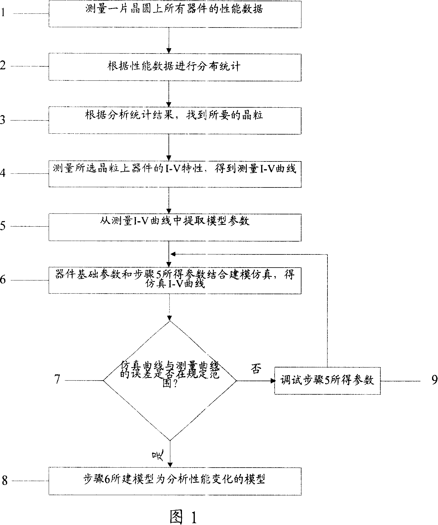
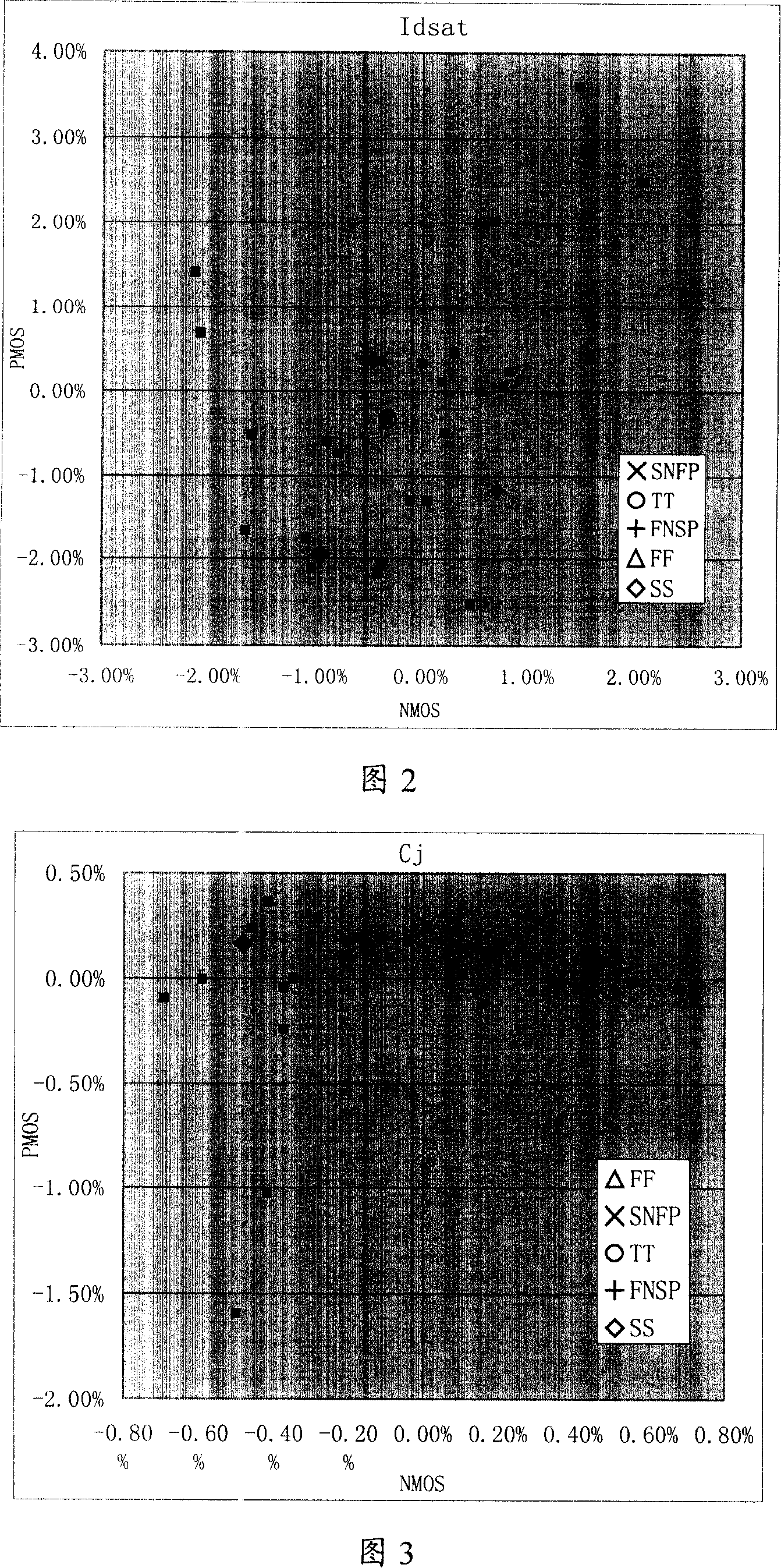
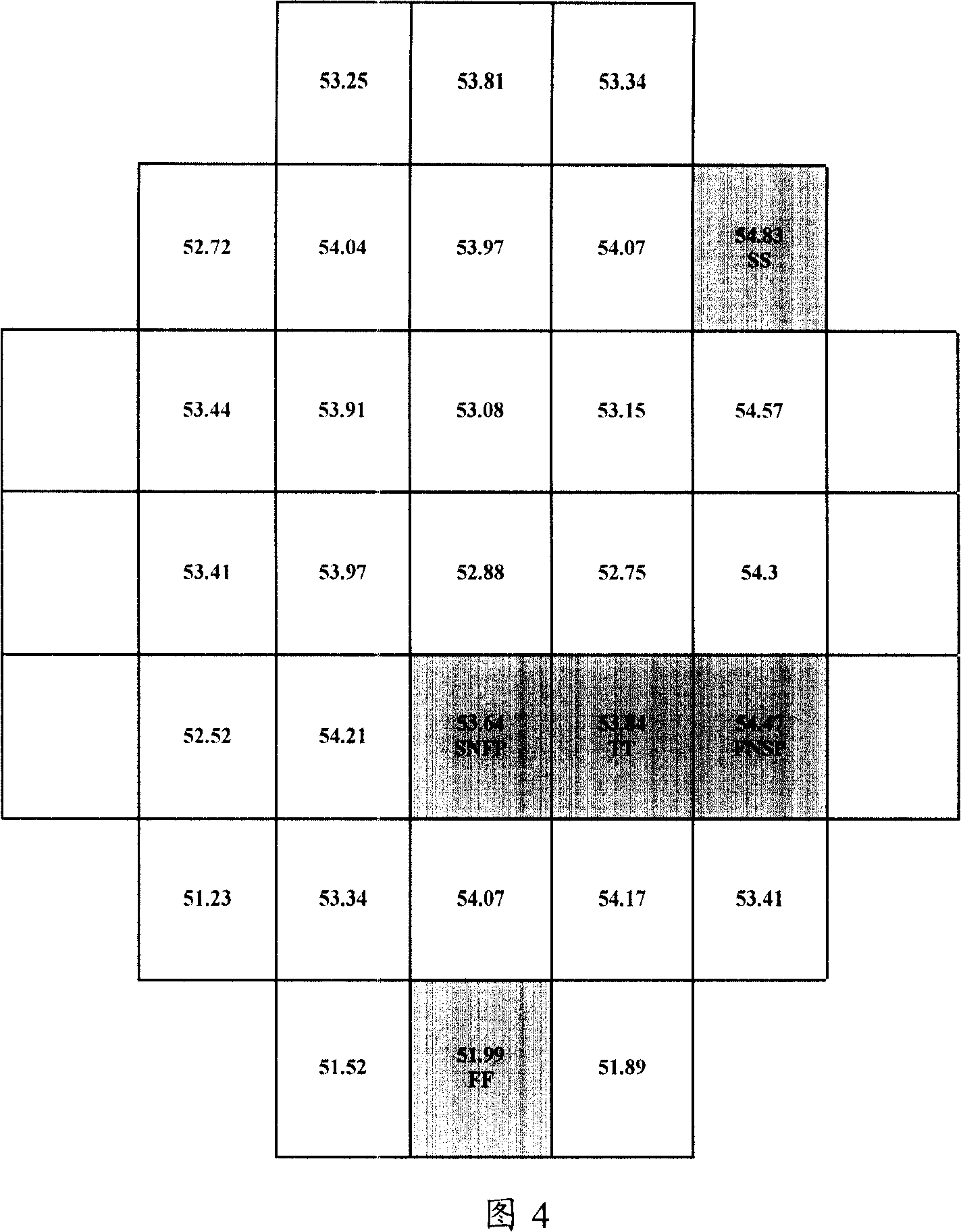
[0015] This embodiment is modeled by the modeling method disclosed in the present invention: measure the performance data of all transistors on the wafer, perform distribution statistics on the performance data to obtain the grains where some of the largest discrete points are located, and measure the I-V of all transistors in the selected grains The characteristics are measured I-V curves, model parameters are extracted from the measured I-V curves, the model parameters are combined with the transistor basic parameters and input into the simulation software for modeling and simulation to obtain simulated I-V curves, and the model parameters are adjusted so that the error between the simulated I-V curve and the measured I-V curve is within Within the specified range, the model used for the simulation curve that finally meets the error requirements is used as the model for performance analysis.

[0016] In this embodiment, one wafer is used. There are 31 crystal grains on the w...


PUM


Abstract

The present invention discloses a building device model method based on the change of integrated circuit manufacturing procedure performance. Firstly, performance data of all transistors on a wafer are measured; crystal grains of a plurality of biggest discrete points are obtained by distributing statistics on the performance data. Then I-V properties of all the transistors of all crystal grains are measured to obtain a measuring I-V curve; model parameters are extracted from the measuring I-V curve. Next, the model parameters combining with the basic parameters of the transistors are input into a simulation software to obtain a simulation I-V curve through model building and simulation; the model parameters are debugged to make errors of the simulation I-V curve and the measuring I-V curve in a specified scope; finally the model satisfying the need of error is used as a performance-analysis model. Models produced by the model building method of the invention can reflect the scope of the device performance on the wafer deviating from a predicated value or a medium value more accurately, thereby helping designers predict the fluctuation of production technique and the deviation of device dimension.

Description

technical field [0001] The invention relates to a method for simulating the performance change of an integrated circuit manufacturing process, in particular to a method for establishing a model required for the simulation. Background technique [0002] In the integrated circuit manufacturing process, there will be process fluctuations and device size reduction, which will lead to unstable device or circuit performance. Therefore it is necessary to verify whether the product works as expected. For example, what is the performance of the product and what is the statistical distribution of the performance? The simulation results of these indicators will have a feedback effect on the process. Based on this, accurately reflecting the variation of process performance is an important issue of concern today. Therefore, a method of reflecting performance changes through discrete case model simulation is derived. A good modeling method should not only be able to accurately reflect ...

Claims


Application Information

Patent Timeline
IPC IPC(8): G06F17/50
Inventor 陈良成刘鉴常包自意余泳
Owner SEMICON MFG INT (SHANGHAI) CORP
Learn More