Printed circuit board

A technology for wiring circuit substrates and dielectric constants, which can be applied to printed circuits, printed circuits, circuit devices, etc., and can solve problems such as loss and reduced signal transmission efficiency.

Inactive Publication Date: 2008-04-02
NITTO DENKO CORP
View PDF1 Cites 0 Cited by
  • Summary
  • Abstract
  • Description
  • Claims
  • Application Information

AI Technical Summary

Problems solved by technology

As a result, loss occurs in the transmission path of the printed circuit board, and the signal transmission efficiency decreases

Method used


Image

  • Printed circuit board
  • Printed circuit board
  • Printed circuit board

Examples


Embodiment Construction

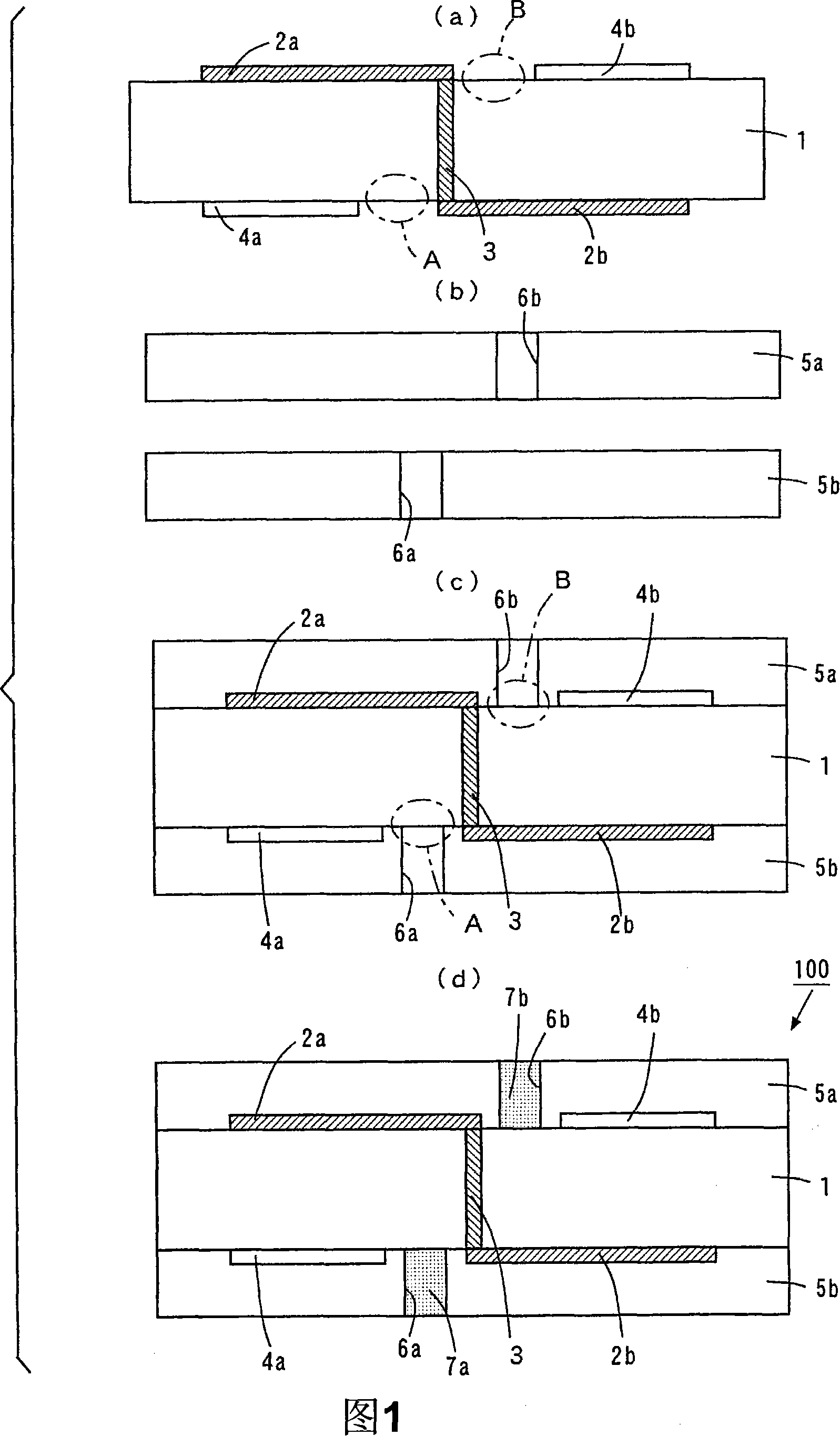
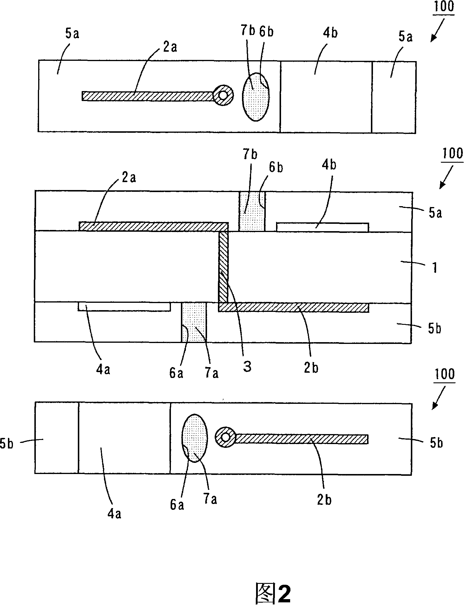
[0033] Hereinafter, a printed circuit board according to an embodiment of the present invention will be described with reference to the drawings. The printed circuit board of this embodiment is a flexible printed circuit board.

[0034] (1) Manufacturing method of printed circuit board

[0035] FIG. 1 is a schematic process cross-sectional view showing an example of a method of manufacturing a printed circuit board according to the present embodiment.

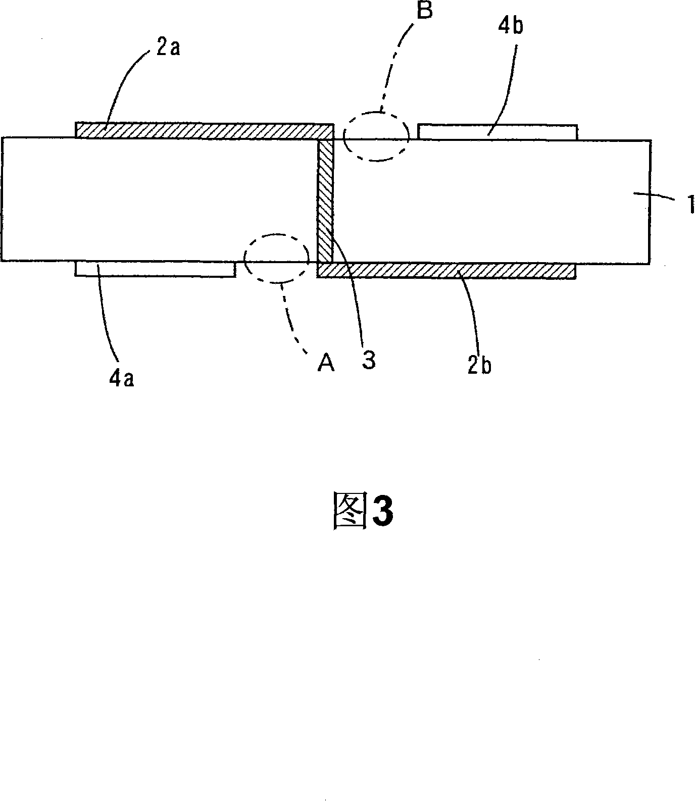
[0036] As shown in FIG. 1(a), predetermined wiring patterns 2a, 2b made of, for example, copper are respectively formed on one side and the other side of an insulating base layer 1 made of, for example, a polyimide film. In addition, base insulating layer 1 made of epoxy resin, acrylic resin, or butyral resin may also be used. In addition, the specific dielectric constant of the insulating base layer 1 is, for example, approximately 3.2 to 4.0.

[0037] In addition, a metal plating layer 3 for electrically connecting the abo...


PUM


Abstract

A first wiring pattern and a second ground layer are formed on one surface of a base insulating layer, and a second wiring pattern and a first ground layer are formed on the other surface of the base insulating layer. A metal plating layer connecting the first and second wiring patterns to each other is formed in a through hole of the base insulating layer. A cover insulating layer is formed on the other surface of the base insulating layer so as to cover the first ground layer and the second wiring pattern and has a through hole on an area opposite to a part of the first wiring pattern. A high dielectric insulator is formed in the through hole of the cover insulating layer.

Description

technical field [0001] The present invention relates to a printed circuit board used in various electric equipment or electronic equipment. Background technique [0002] Conventionally, printed circuit boards (printed wiring boards) have been used in various electric and electronic devices. In order to realize miniaturization and weight reduction of electric and electronic equipment, electronic components are mounted on the miniaturized printed circuit board while increasing the density of wiring patterns on the printed circuit board. [0003] In recent years, as described above, in order to further increase the density and reduce the size of a printed circuit board, a printed circuit board having a multilayer structure has been developed (for example, refer to Japanese Patent Application Laid-Open No. 2000-323847). [0004] Conventional printed circuit boards have the following problems. FIG. 3 is a schematic cross-sectional view schematically showing the structure of a c...

Claims


Application Information

Patent Timeline
Patent Type & Authority Applications(China)
IPC IPC(8): H05K1/02H05K3/46
CPCH05K3/4644H05K1/162H05K1/024H05K2201/0187H05K2203/063H05K1/115H05K2201/09336H05K2201/09536H05K2201/0209
Inventor 本上满
Owner NITTO DENKO CORP
Why Eureka
Try Eureka