Liquid crystal display

A liquid crystal display device and liquid crystal layer technology, applied in static indicators, nonlinear optics, instruments, etc., can solve the problem of power consumption of the display device, such as the area of ​​the coloring layer, and achieve the effects of improving display effects, saving power consumption, and increasing the area

Inactive Publication Date: 2008-04-23
INNOCOM TECH SHENZHEN +1
View PDF0 Cites 14 Cited by
  • Summary
  • Abstract
  • Description
  • Claims
  • Application Information

AI Technical Summary

Problems solved by technology

[0008] In order to solve the problem that the liquid crystal display device in the prior art consumes more power and the area of ​​the colored la

Method used


Image

  • Liquid crystal display
  • Liquid crystal display
  • Liquid crystal display

Examples


Example Embodiment

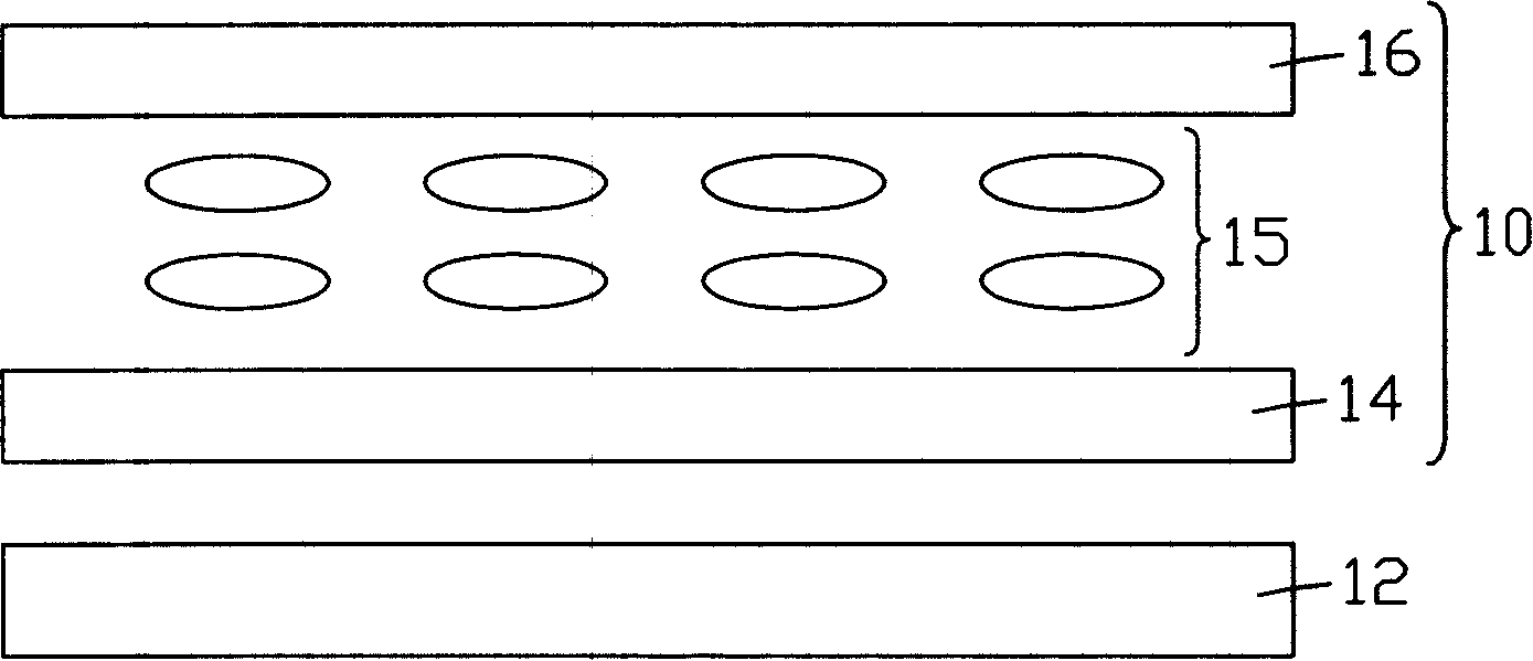
[0019] see Figure 4 , is a schematic diagram of the first embodiment of the liquid crystal display device of the present invention. The liquid crystal display device 2 includes a liquid crystal panel 20 and a backlight module 22 . The liquid crystal panel 20 includes a first substrate 24 , a second substrate 26 corresponding to the first substrate 24 , and a liquid crystal layer 25 filled between the two substrates 24 and 26 . The backlight module 22 is disposed adjacent to the first substrate 24 .

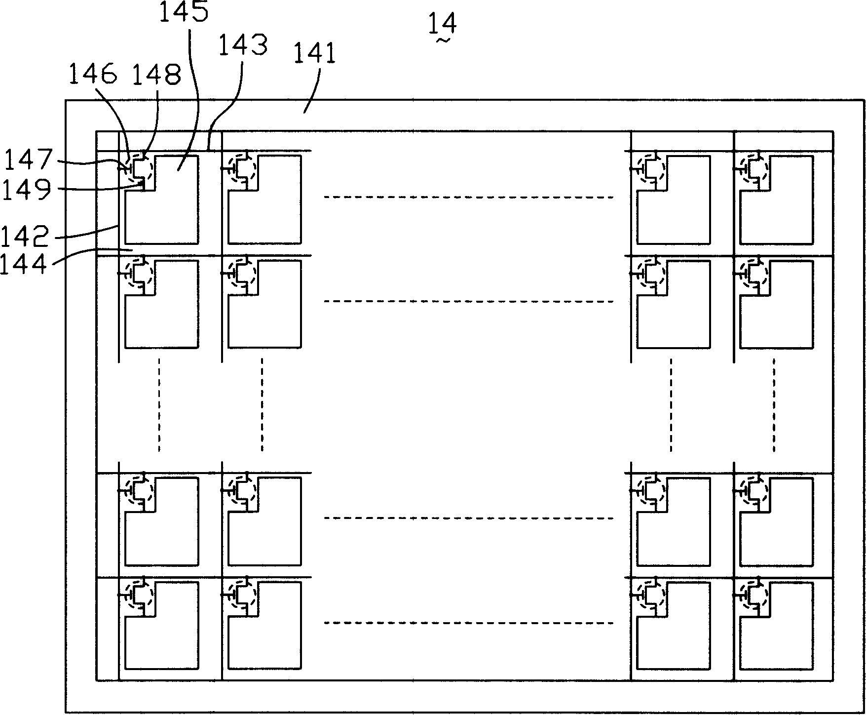
[0020] Please also refer to Figure 5 , is a schematic diagram of the first substrate 24 . The first substrate 24 includes a first base 241 , a plurality of scan lines 242 arranged parallel to each other on the first base 241 , a plurality of data lines 243 parallel to each other and perpendicular to the scan lines 242 , a plurality of data lines 243 located in the scan line 242 Thin film transistors 246 , a plurality of pixel electrodes 245 , a reflective layer 247 , a color...


PUM


Abstract

The LCD display device comprises a first baseboard, a second baseboard corresponding to said first baseboard, a liquid crystal layer located between the two baseboards and a backlight module closed to the first baseboard. The first baseboard comprises a first base, multi scan parallel lines located at said base; multi parallel data lines normal to the scan lines, multi thin film transistors located at intersections between the scan line and data lines, a reflection layer and a color filter layer located at the reflection layer; the minimum area around by the scan lines and the data lines is defined as a pixel unit; the reflection layer covers the thin film transistor. Said color filter layer comprises a colored layer and a black matrix; said colored layer corresponds to the pixel unit; said black matrix corresponds to the scan lines and the data lines.

Description

technical field [0001] The invention relates to a liquid crystal display device. Background technique [0002] Liquid crystal display devices are widely used because of their low radiation, light, thin and small size, and low power consumption. [0003] see figure 1 , is a schematic diagram of a liquid crystal display device in the prior art. The liquid crystal display device 1 includes a liquid crystal panel 10 and a backlight module 12 arranged opposite to the liquid crystal panel 10. The liquid crystal panel 10 includes a first substrate 14 opposite to the first The substrate 14 is provided with a second substrate 16 and a liquid crystal layer 15 filled between the two substrates. The backlight module 12 is disposed adjacent to the first substrate 14 . [0004] Please also refer to figure 2 , is a schematic diagram of the first substrate 14 . The first substrate 14 includes a first base 141, a plurality of scanning lines 142 arranged parallel to each other on the fi...

Claims


Application Information

Patent Timeline
IPC IPC(8): G02F1/136G02F1/1335G02F1/1337G02F1/133
Inventor 周伟黄丽娟
Owner INNOCOM TECH SHENZHEN
Why Eureka
Try Eureka