Multi-chip stack packaging structure with asymmetric conductive wire rack

A technology of chip packaging and stacking structure, applied in the field of multi-chip stacking packaging structure, can solve problems such as electrical signal phase change, metal wire displacement, chip short circuit, etc.

Active Publication Date: 2008-05-07
CHIPMOS TECH INC
View PDF0 Cites 8 Cited by
  • Summary
  • Abstract
  • Description
  • Claims
  • Application Information

AI Technical Summary

Problems solved by technology

[0004] In the above-mentioned known chip stack package structure, since the metal wires 10, 11, 12 between each chip and the platform portion 5c of the lead frame 5 have different lengths and radians, the length and radian are not the same except durin

Method used


Image

  • Multi-chip stack packaging structure with asymmetric conductive wire rack
  • Multi-chip stack packaging structure with asymmetric conductive wire rack
  • Multi-chip stack packaging structure with asymmetric conductive wire rack

Examples


Embodiment approach

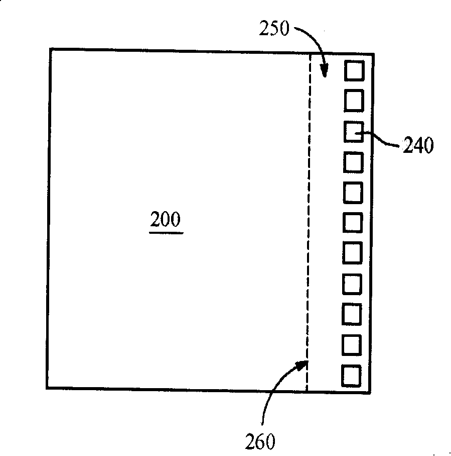
[0073] as reference Figure 2A and Figure 2B As shown, a schematic plan view and a schematic cross-sectional view of the chip 200 that has completed the aforementioned process. Such as Figure 2B As shown, the chip 200 has an active surface 210 and a back surface 220 opposite to the active surface, and an adhesive layer 230 has been formed on the back surface 220 of the chip; it should be emphasized here that the adhesive layer 230 of the present invention is not limited to the aforementioned prepreg. The purpose of the adhesive layer 230 is to form a bond with the substrate or the chip. Therefore, as long as it is an adhesive material with this function, it is an embodiment of the present invention, such as a die attached film.

[0074] Next, please refer to Figure 2C , a schematic cross-sectional view of a multi-chip offset stack structure 30 completed by the present invention. Such as Figure 2C As shown, a plurality of welding pads 240 are arranged on the active sur...


PUM


Abstract

The invention relates to a stacked chip packaging structure, comprising a wire rack, wherein, the wire rack comprises a plurality of internal pins and a plurality of external pins; the internal pins comprise a plurality of first parallel internal pin clusters and second parallel internal pin clusters, the tail ends of the first internal pin clusters and the second internal pin clusters are arranged oppositely with an interval; the tail ends of the first internal pin clusters and the tail ends of the second internal pin clusters have different vertical height due to the sink-arranged structure of the first internal pin clusters; the multi-chip stacked structure is connected fixedly with the first internal pin clusters; the metal welding points on the edge of the same side of the multi-chip stacking structure are connected electrically with the first internal pin clusters and the second internal pin clusters via a plurality of metal wires; the multi-chip stacked structure and the internal pins are packaged with sealant; and the packaging structure is provided with a top surface and a bottom surface.

Description

technical field [0001] The invention relates to a multi-chip stack packaging structure, in particular to a multi-chip stack packaging structure using lead frames with inner leads of different heights. Background technique [0002] In recent years, three-dimensional space (Three Dimension; 3D) packaging is being carried out in the back-end process of semiconductors, in order to achieve higher density or memory capacity with the least area. In order to achieve this goal, a chip stacked method has been developed to achieve a three-dimensional (Three Dimension; 3D) package at this stage. [0003] In the known technology, the chip stacking method is to stack multiple chips on the substrate, and then use a wire bonding process to connect the multiple chips to the substrate. Figure 1 discloses a structure of a chip stack package based on a lead frame, wherein Figure 1A for a cross-sectional diagram Figure 1B for Figure 1A floor plan. Such as Figure 1A As shown, the lead fram...

Claims


Application Information

Patent Timeline
IPC IPC(8): H01L25/00H01L25/065H01L23/488H01L23/495
CPCH01L2224/32245H01L2224/73265H01L2224/48247H01L2224/32145H01L2225/06562H01L2224/48145H01L24/73H01L2924/181
Inventor 沈更新杜武昌
Owner CHIPMOS TECH INC
Why Eureka
Try Eureka