

Low voltage complementary metal oxide semiconductor process tri-state buffer
An oxide semiconductor and tri-state buffer technology, applied in the field of buffers, can solve the problems of limited size, power consumption, and long voltage level drop time
- Summary
- Abstract
- Description
- Claims
- Application Information
AI Technical Summary
Problems solved by technology
Method used
Image

Examples
Embodiment Construction
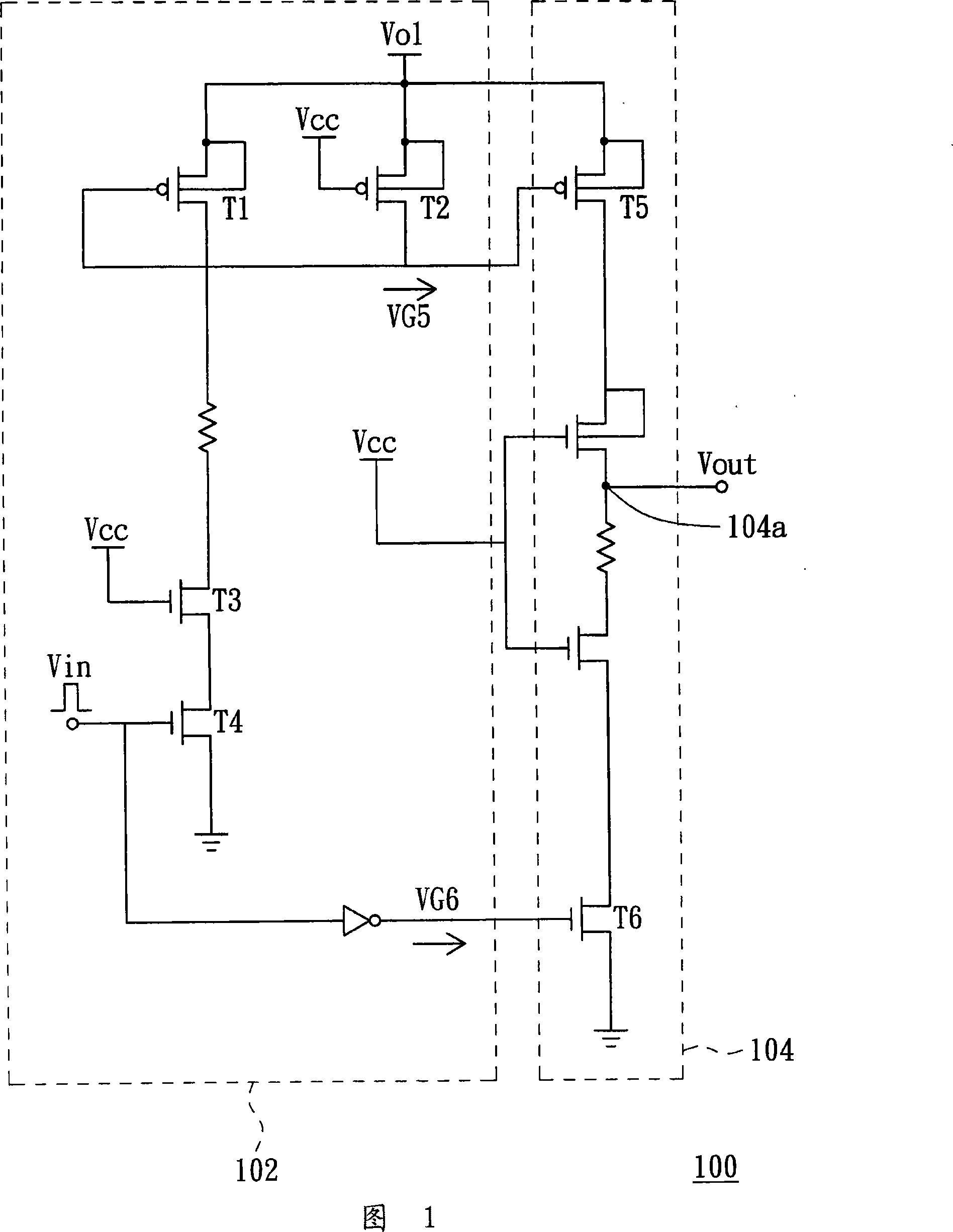
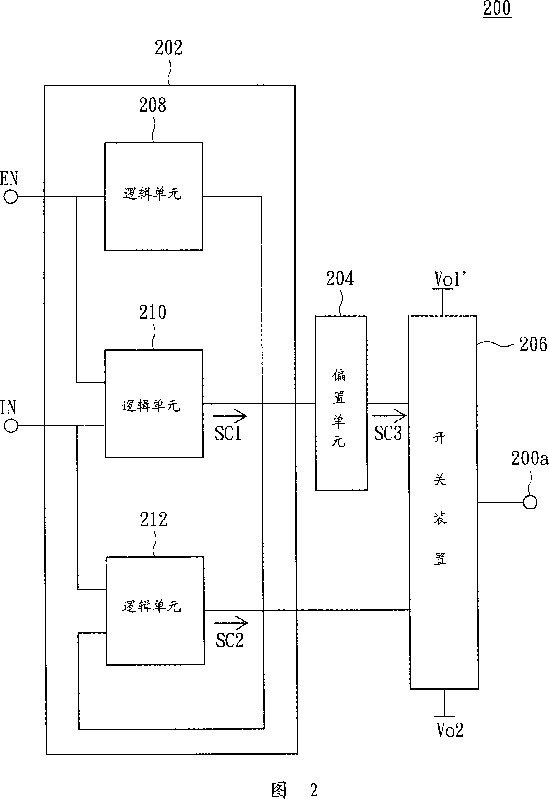
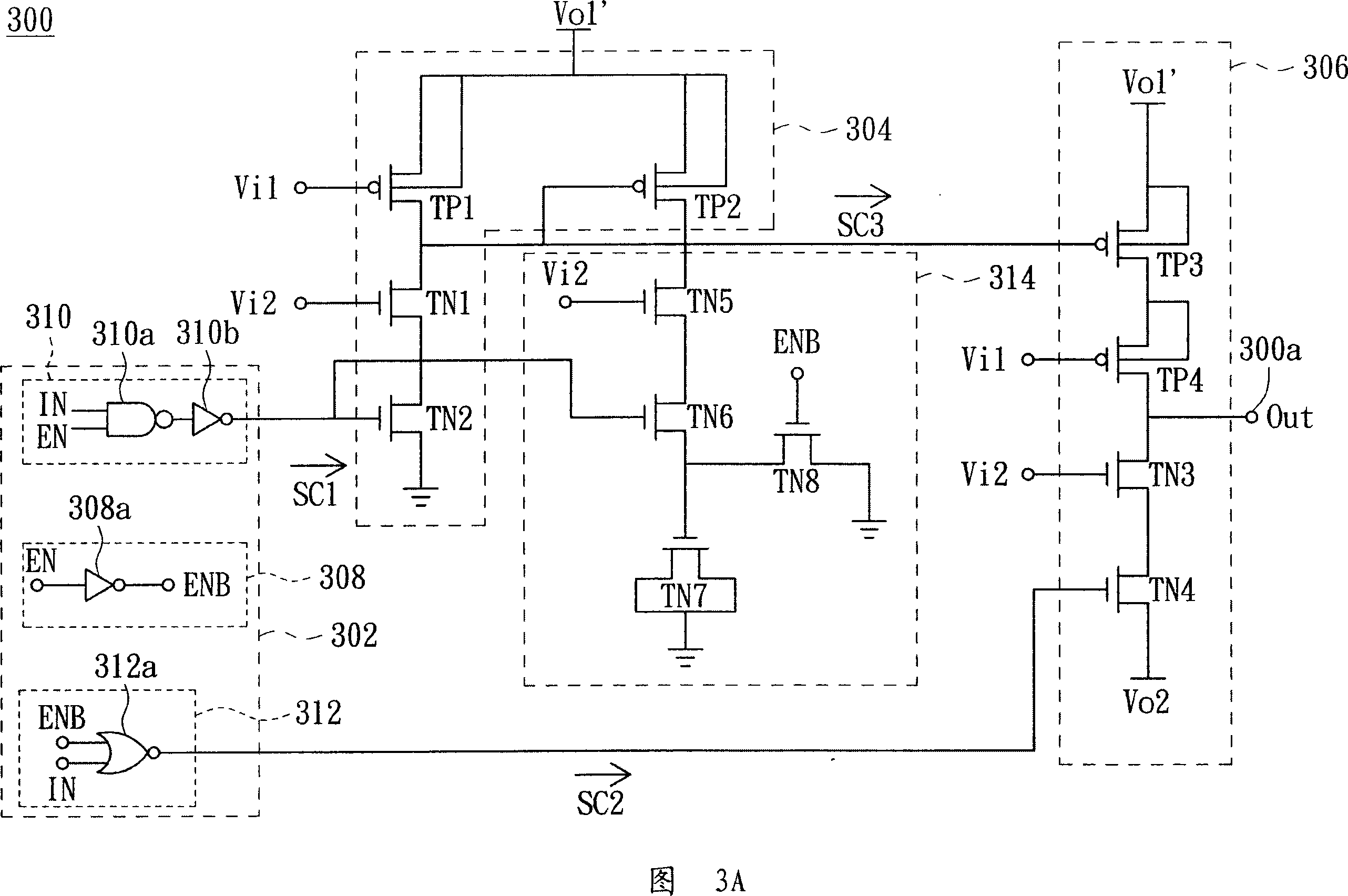
[0032] A tri-state buffer (Tri-State Buffer) made of low-voltage complementary metal oxide semiconductor (Complementary Metal Oxide Semiconductor, CMOS), including a logic device, a bias device and a switch device. The logic device receives the input signal and the enabling signal and generates a first control signal and a second control signal accordingly. The bias device receives the first control signal and controls the signal level of the third control signal accordingly. The switch device receives the second and third control signals, and is respectively coupled to the output terminal to the first external voltage terminal and the second external voltage terminal when the second and third control signals are enabled. Wherein, when the enabling signal is disabled, the second and third control signals are simultaneously disabled, so that the output terminal is simultaneously floating with the first and second external voltage terminals, and the output terminal is in a high-...
PUM
 Abstract
Description
Claims
Application Information