Flash memory device and method for controlling the same

A flash memory, erasing voltage technology, applied in the field of flash memory devices

Active Publication Date: 2008-05-14
SK HYNIX INC
View PDF0 Cites 16 Cited by
  • Summary
  • Abstract
  • Description
  • Claims
  • Application Information

AI Technical Summary

Problems solved by technology

If the erase operation is not implemented properly, the corresponding block will be marked as an invalid block that is not used

Method used


Image

  • Flash memory device and method for controlling the same
  • Flash memory device and method for controlling the same
  • Flash memory device and method for controlling the same

Examples


Embodiment Construction

[0050] Now, various embodiments according to the present invention will be described with reference to the accompanying drawings. Since various embodiments are proposed so that those skilled in the art can understand the present invention, it can be modified in various ways and various embodiments described later do not limit the scope of the present invention.

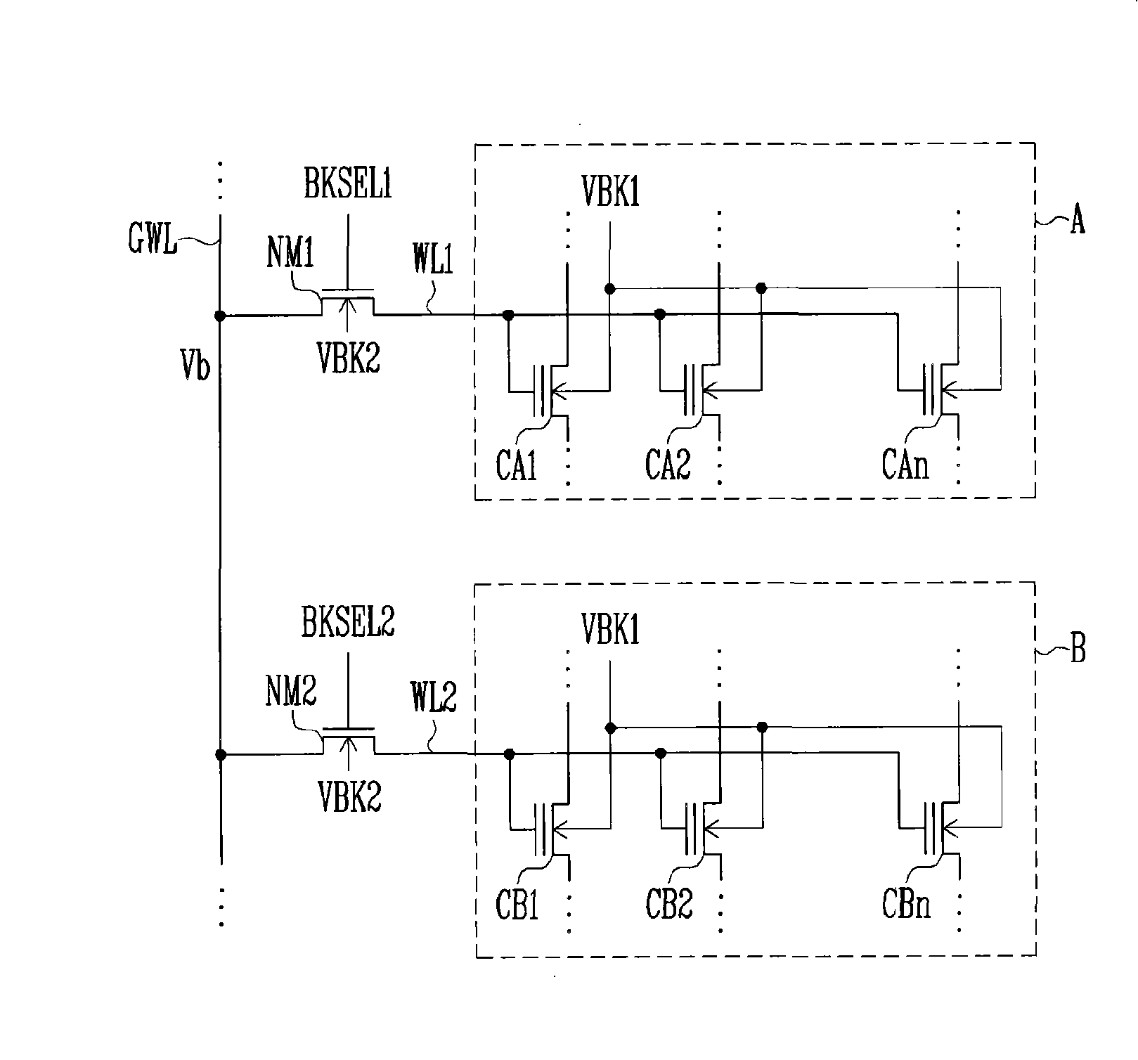
[0051]FIG. 4 is a block diagram of a flash memory device according to an embodiment of the invention. The flash memory device 100 includes a memory cell array 110, an input buffer 120, a control logic circuit 130, a high voltage generator 140, an X-decoder 150, a block selection unit 160, a page buffer 170, a Y-decoder 180, and a data I / O buffer 190. The memory cell array 110 includes memory cell blocks MB1 to MBK (where K is an integer), and each memory cell block has a plurality of memory cells (not shown). The input buffer 120 receives the command signal CMD or the address signal ADD, and outputs them to the con...


PUM


Abstract

The present invention provides a flash memory device and a method used for controlling erasing operation of the flash memory device.A non-volatile memory mechanism includes a first and a second memory cell blocks, wherein each memory cell block includes a plurality of memory cells, a local drain selection wire, a local source pole selection wire and a plurality of local character wires.A block selection unit respectively connects the set local character wires and an integral character wire to respond to block selective signals.A first voltage bias generator is allocated to be used for applying at least a first and a second erasing voltages which are positive ones to the integral character wire during the erasing manipulation period, wherein, the first erasing voltage is applied to the integral character wire during a first erasing try period of the erasing operation, the second erasing voltage is applied to the integral character wire during the second erasing try period, and a second erasing try is executed if a first erasing try does not make good erasing manipulation.A body voltage generator applies a body electric voltage to a body of the memory cell during the erasing manipulation period.

Description

technical field [0001] The present invention relates to a semiconductor memory device, and more particularly, to a flash memory device in which the reliability of an erase operation due to leakage current in a block-based erase operation can be prevented from being reduced, and to controlling the flash memory device method of the erase operation. Background technique [0002] Generally, flash memory devices can be classified into NOR type and NAND type, wherein the NOR type is generally used to store a small amount of information at high speed, and the NAND type is generally used to store a large amount of information. The flash memory device performs a read operation, a program operation, and an erase operation. The terms "program operation" and "erase operation" refer to the process of storing and storing data in one or more memory cells by injecting electrons into and removing electrons from the floating gate. Data manipulation. For example, in a program operation, onl...

Claims


Application Information

Patent Timeline
Patent Type & Authority Applications(China)
IPC IPC(8): G11C16/16G11C16/08
CPCG11C16/0483G11C16/16
Inventor 李熙烈
Owner SK HYNIX INC
Why Eureka
Try Eureka