Nitride semiconductor light emitting element

A technology of nitride semiconductors and light-emitting elements, which is applied in the direction of semiconductor devices, semiconductor lasers, and electrical components, and can solve problems such as complex manufacturing processes, reduced luminous output, and increased resistance of electrode connections

Inactive Publication Date: 2008-05-14
ROHM CO LTD
View PDF1 Cites 5 Cited by
  • Summary
  • Abstract
  • Description
  • Claims
  • Application Information

AI Technical Summary

Problems solved by technology

Therefore, the manufacturing process becomes very complicated, and contamination generated by etching adheres to the light-emitting surface, the electrode-formed surface, etc., and there are also problems with electrical characteristics such as a decrease in light-emitting output and an increase in the resistance of the electrode connection part.

Method used


Image

  • Nitride semiconductor light emitting element
  • Nitride semiconductor light emitting element

Examples


Embodiment Construction

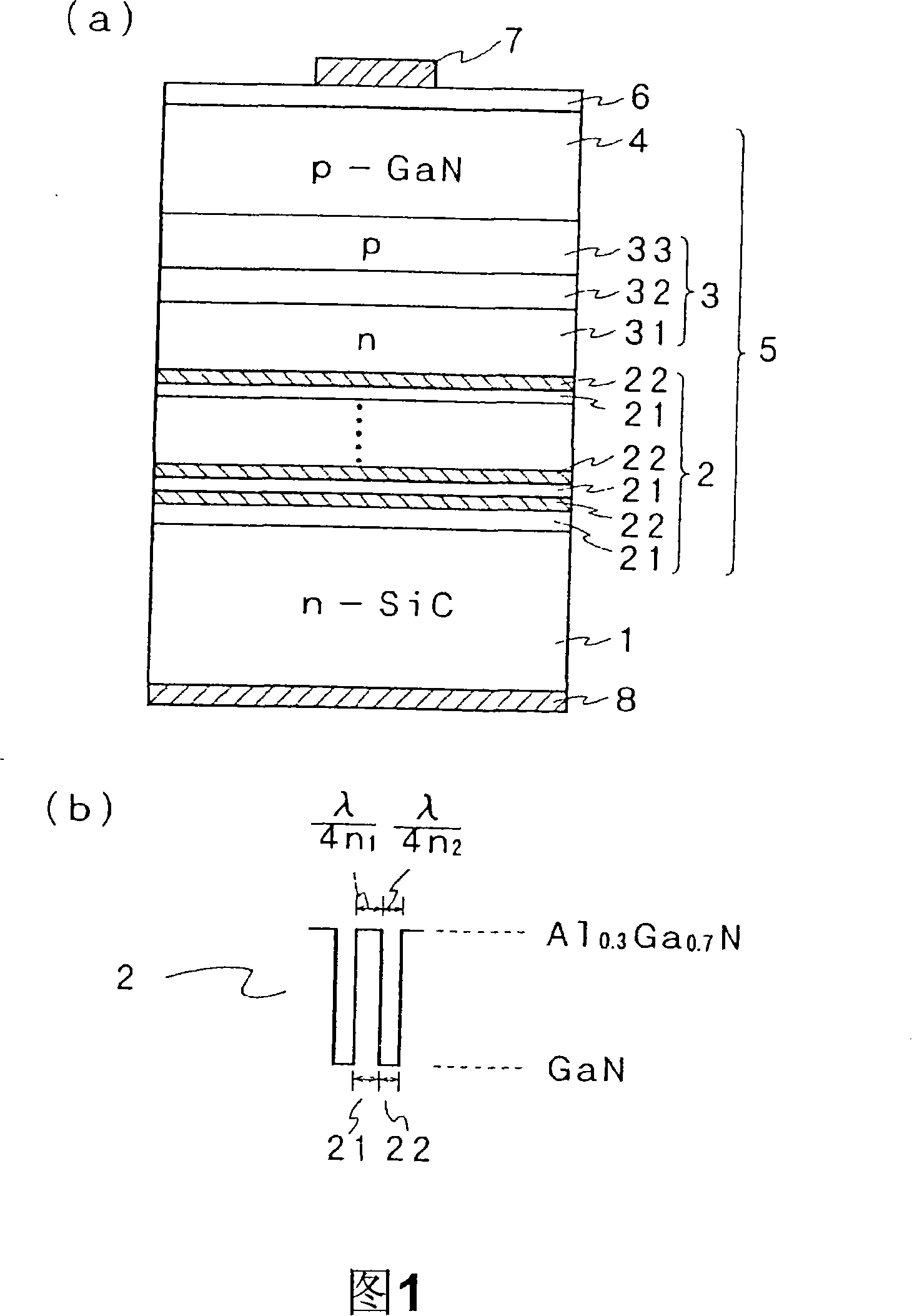
[0033] Next, the nitride semiconductor light-emitting device of the present invention will be described with reference to the drawings. The nitride semiconductor light-emitting element of the present invention, an explanatory cross-sectional view of one embodiment thereof and an energy band diagram of the light reflection layer are shown in FIG. The light reflection layers 2 are laminated alternately with the high refractive index layers 22 , and on the light reflection layers 2 are provided semiconductor lamination portions 5 in which nitride semiconductor layers are laminated so as to have at least the light emitting layer formation portion 3 . It is formed by providing the upper electrode 7 on the upper surface side of the semiconductor laminated portion 5 and the lower electrode 8 on the back surface of the SiC substrate 1 .

[0034] SiC substrate 1 uses a single crystal silicon carbide substrate, and is formed in n-type in the example shown in FIG. 1 . A light reflection...


PUM


Abstract

The invention provides a nitride semiconductor light emitting element wherein emission output deterioration due to film quality deterioration of a nitride semiconductor layer due to lattice mismatch between a substrate and the nitride semiconductor layer is prevented and light traveling to the substrate can be also efficiently used, while permitting the light emitting element to be a vertical type, by using the SiC substrate. A light reflecting layer (2) wherein low refractive index layers (21) and high refractive index layers (22) having different refractive indexes are alternately stacked is directly arranged on the SiC substrate (1). On the light reflecting layer (2), a semiconductor multilayer section (5) wherein a nitride semiconductor layer is stacked to have at least a light emitting layer forming section (3) is arranged on the light reflecting layer (2). On an upper plane side of the semiconductor multilayer section (5), an upper electrode (7) is arranged, and on a rear plane of the SiC substrate (1), a lower electrode (8) is arranged.

Description

technical field [0001] The present invention relates to a semiconductor light emitting element using a nitride semiconductor. More specifically, it relates to a nitride semiconductor luminescence that uses a semiconductor substrate made of SiC as a substrate, provides an electrode on the back surface of the substrate, and can efficiently extract light emitted from a light-emitting layer forming part, thereby improving the external quantum efficiency. element. Background technique [0002] In the conventional semiconductor light-emitting element using a nitride semiconductor, for example, a nitride semiconductor laminate including a buffer layer and a light-emitting layer forming portion is grown on a sapphire substrate, and a part of the semiconductor laminate is etched to make the semiconductor laminate The conductive layer on the lower layer side is exposed, and a lower electrode is provided on the surface of the exposed lower conductive layer, and an upper electrode is p...

Claims


Application Information

Patent Timeline
Patent Type & Authority Applications(China)
IPC IPC(8): H01L33/00H01S5/183H01L33/06H01L33/10H01L33/32H01L33/42
CPCH01L33/10H01L33/32H01S5/187H01S5/32341
Inventor 田中治夫园部雅之
Owner ROHM CO LTD
Why Eureka
Try Eureka