Illumination device with semiconductor light-emitting elements

A technology for lighting devices and light-emitting elements, which is applied to semiconductor devices, semiconductor/solid-state device parts, electrical components, etc., can solve problems such as insufficient utilization and insufficient brightness, and achieve the effect of preventing temperature rise

Inactive Publication Date: 2008-06-04
TOSHIBA LIGHTING & TECH CORP
View PDF6 Cites 31 Cited by
  • Summary
  • Abstract
  • Description
  • Claims
  • Application Information

AI Technical Summary

Problems solved by technology

Therefore, insufficient utilization of the light emitted from the LED chip may resu

Method used


Image

  • Illumination device with semiconductor light-emitting elements
  • Illumination device with semiconductor light-emitting elements
  • Illumination device with semiconductor light-emitting elements

Examples


Embodiment Construction

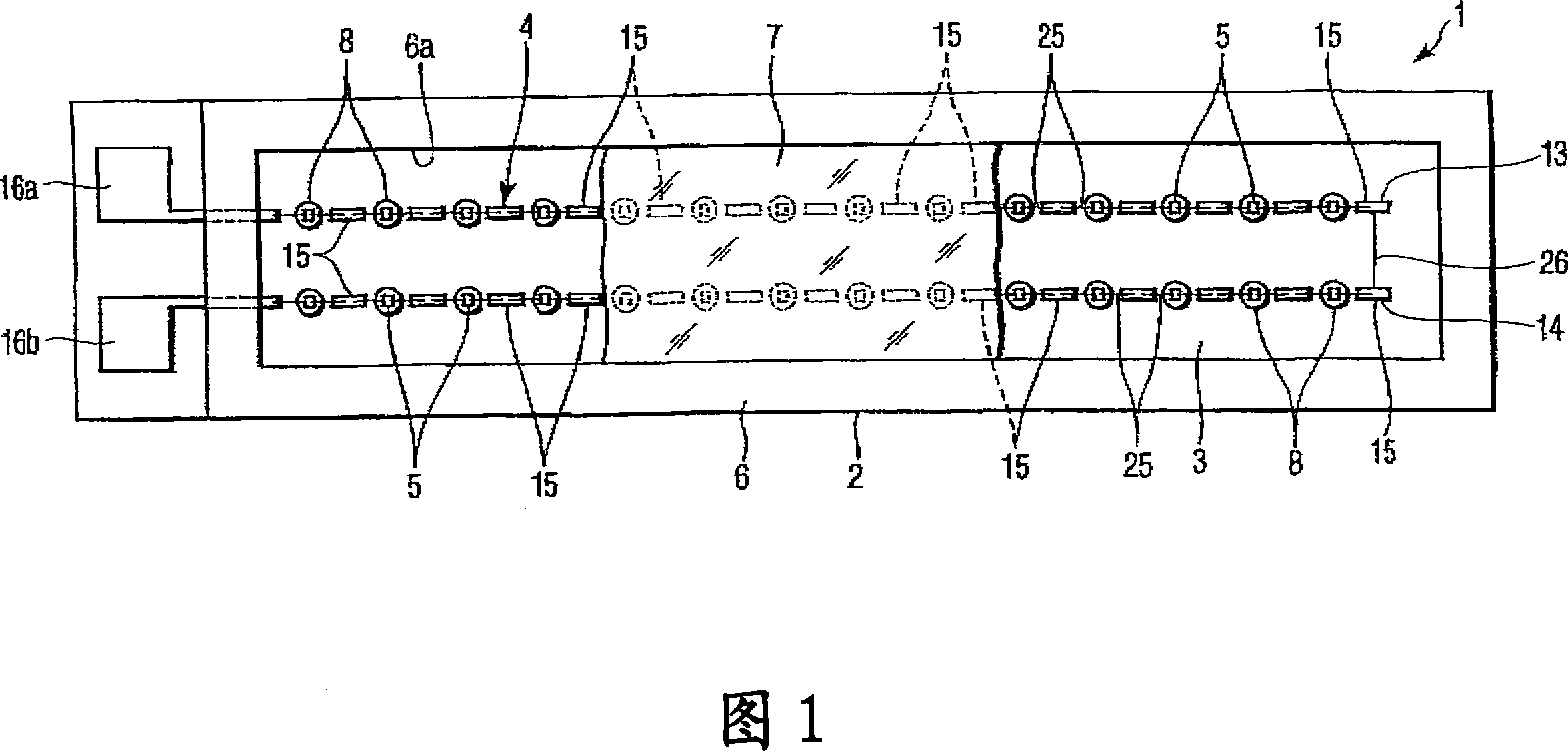
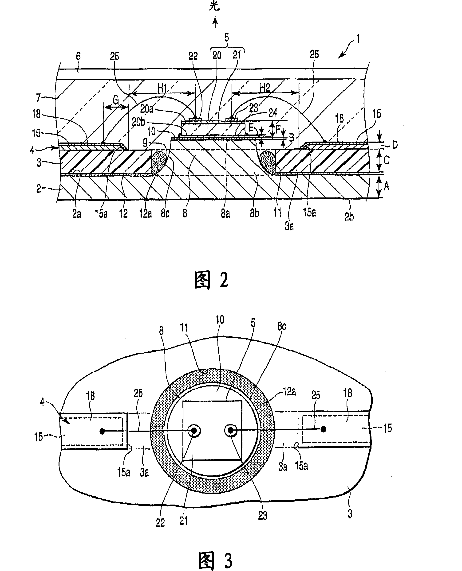
[0107] A first embodiment of the present invention will be described below with reference to FIGS. 1 to 5 .

[0108] Fig. 1 discloses a lighting device 1 eg forming an LED package. The lighting device 1 includes a baseboard 2 , an insulating layer 3 , a conductive pattern 4 , a plurality of semiconductor light emitting elements 5 , a reflector 6 , and a sealing member 7 .

[0109] The substrate 2 has, for example, a rectangular shape in order to obtain a light emitting area necessary for the lighting device 1 . As the material of the substrate 2, it is desirable to use a metal excellent in heat dissipation, such as copper and aluminum alloy. As shown in FIG. 2 , the substrate 2 has a front surface 2 a and a rear surface 2 b located on the opposite side of the front surface 2 a. A plurality of cylindrical protrusions 8 are integrally formed on the front surface 2 a of the substrate 2 . The number of protrusions 8 corresponds to the number of semiconductor light emitting elem...


PUM

PropertyMeasurementUnit
Thicknessaaaaaaaaaa

Abstract

An illumination device includes a base board, an insulator, a conductor, a plurality of semiconductor light-emitting elements and a light-transmissive sealing member. The base board includes a surface and projection portions. The projection portion is formed to become gradually thicker from its end toward the surface of the base board. The insulator is formed on the surface. The conductor is formed on the insulator. The semiconductor light-emitting elements are mounted on the projection portions. The semiconductor light-emitting elements are electrically connected to the conductor via connection members. The sealing member covers the insulator, the projection portions, the semiconductor light-emitting elements and the connection members.

Description

[0001] This application is based on and asserts prior Japanese Patent Application No. 2006-324606 filed on November 30, 2006, previous Japanese Patent Application No. 2006-353468 filed on December 27, 2006, March 22, 2007 Previous Japanese Patent Application No. 2007-75637 filed on March 22, 2007, Previous Japanese Patent Application No. 2007-75638 filed on March 22, 2007, Previous Japanese Patent Application No. 2007-82882 filed on March 27, 2007 No., and the benefit of priority of prior Japanese Patent Application No. 2007-250227 filed September 26, 2007, which is incorporated herein by reference in its entirety. technical field [0002] The present invention relates to a lighting device using a plurality of semiconductor light emitting elements such as light emitting diode chips as light sources. Background technique [0003] Japanese Patent Laid-Open No. 2002-94122 discloses a lighting device in which a plurality of LED chips are arranged on a substrate. In this lightin...

Claims


Application Information

Patent Timeline
IPC IPC(8): H01L25/00H01L25/075H01L23/367H01L23/28H01L23/488
CPCH01L2224/48091H01L2224/73265H01L2224/48465
Inventor 三瓶友广林田裕美子泉昌裕大谷清本田豊野木新治
Owner TOSHIBA LIGHTING & TECH CORP
Why Eureka
Try Eureka