Optical short distance amending method

An optical short-distance and distance technology, which is applied in the direction of optics, originals for photomechanical processing, and photoplate-making process on patterned surfaces, can solve the problems of restricting the development of advanced lithography process and the deterioration of imaging results, and achieve improved Effect of graphics resolution and DOF

Active Publication Date: 2008-06-11
SEMICON MFG INT (SHANGHAI) CORP +1
View PDF2 Cites 11 Cited by
  • Summary
  • Abstract
  • Description
  • Claims
  • Application Information

AI Technical Summary

Problems solved by technology

[0006] The existing optical proximity correction method is not suitable for correcting the optical proximity effect within the forbidden pitch range, because the distance between the forbidden pitches is small, which is 120nm to 160nm, and the auxiliary graphics reflected on the photomask parallel to the circuit graphics When it is placed on the semiconductor substrate, the probability of forming a photoresist film pattern corresponding to the auxiliary pattern is very high, resulting in poor imaging results, which severely limits the development of advanced lithography processes.

Method used


Image

  • Optical short distance amending method
  • Optical short distance amending method
  • Optical short distance amending method

Examples


Embodiment Construction

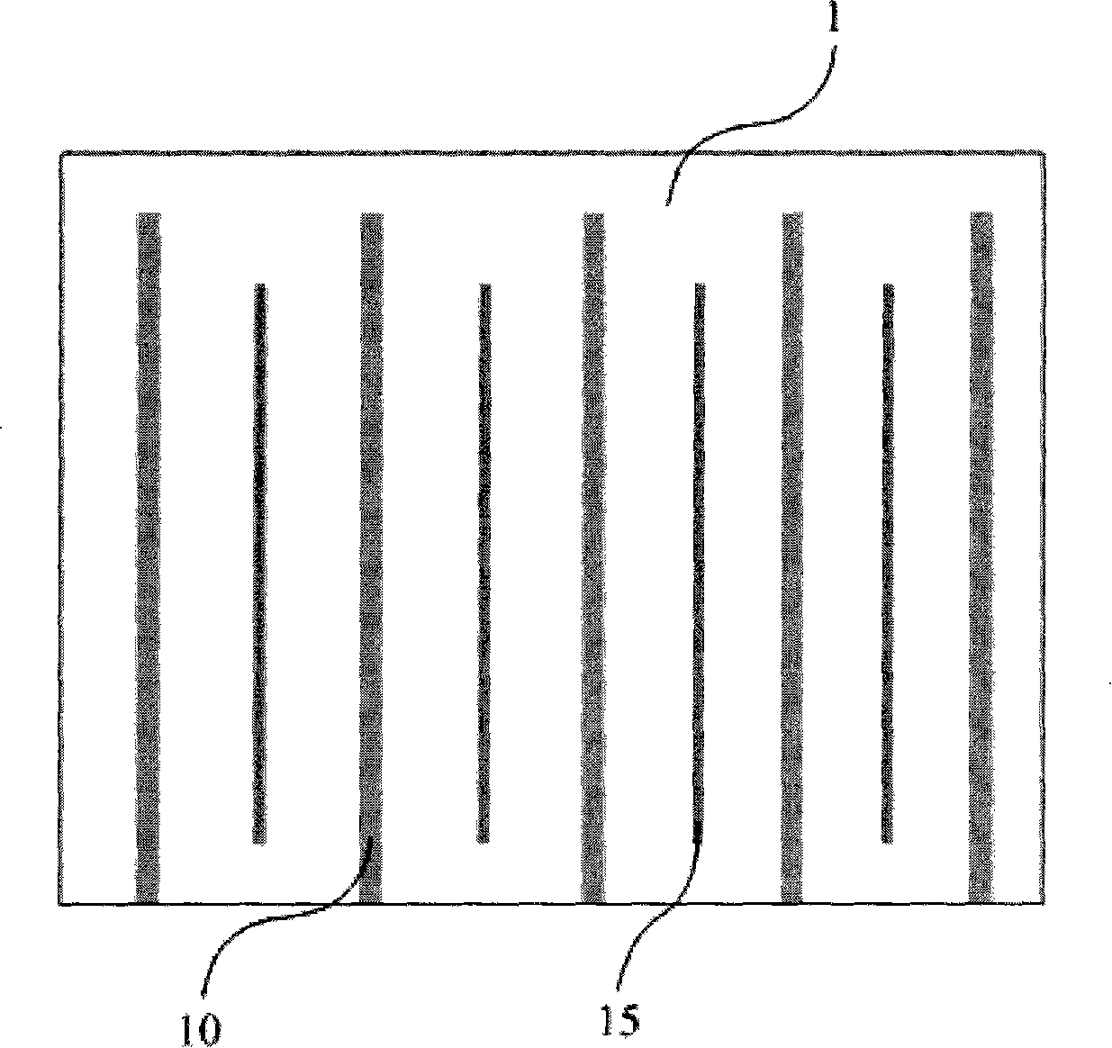
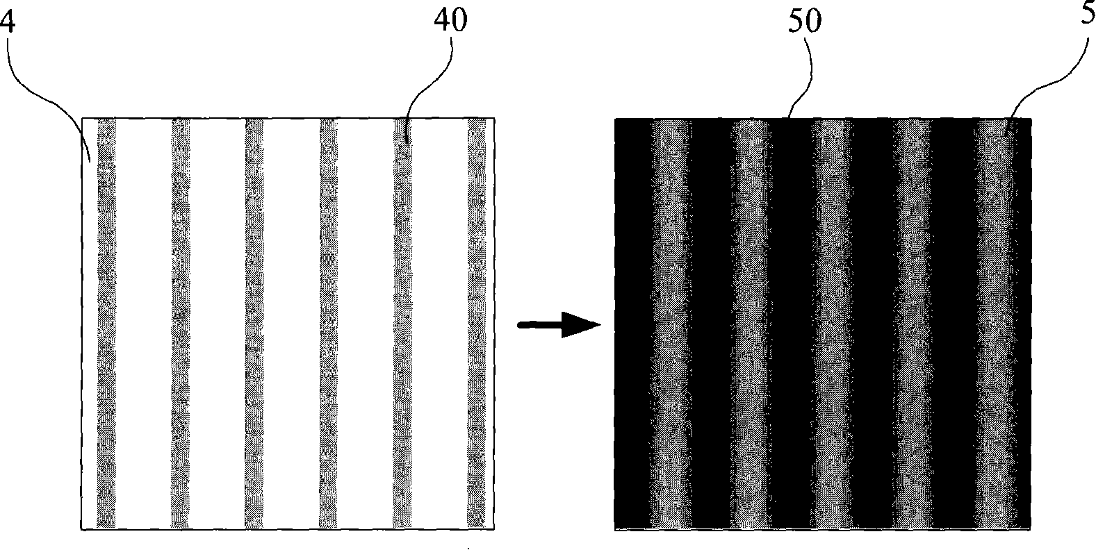
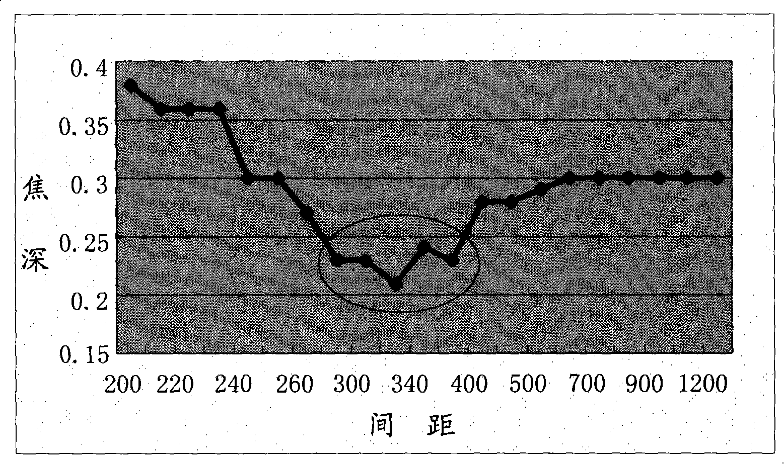
[0023] As integrated circuits contain more and more devices, the size and spacing of individual devices are required to be smaller and smaller. Starting from 0.13 micron products, the optical proximity effect becomes significant, and the optical proximity effect originates from the interference between light scattered on adjacent patterns. Representative optical proximity effects include reduced line width, shortened line ends, and square corner passivation in the forbidden pitch range, which are caused by the decrease of DOF and the increase of MEEF in the forbidden pitch range. of. For processes of 0.13 microns and above, optical proximity correction, including dense and sparse line width balance, line end stability, and square corners plus decorative edges, is sufficient to meet the requirements for line width uniformity. For 0.13 micron and below processes, more complex model-based optical proximity correction becomes indispensable because it can use calibrated optical mo...


PUM

PropertyMeasurementUnit
lengthaaaaaaaaaa
widthaaaaaaaaaa
widthaaaaaaaaaa

Abstract

A method of optics close distance correction is provided, which comprises the following steps: providing at least a circuit figure to be exposed; forming at least one assistant figure to be exposed perpendicular to the circuit figure to be exposed, the dimension of the assistant figure to be exposed is less than the resolution of the lithography machine; transferring the circuit figure to be exposed and the assistant figure to be exposed to the photomask, so as to form the circuit figure and the assistant figure. Through the steps, not only the assistant figure on the photomask perpendicular to the circuit figure can be reflected on the semiconductor underlayer, without forming lithography glue film figure opposite to the assistant figure, so that the imaging effect turns good, but also the figure resolution and DOF are improved.

Description

technical field [0001] The invention relates to the technical field of semiconductor manufacturing, in particular to a method for optical proximity correction (OPC) in a photomask manufacturing process. Background technique [0002] With the rapid development of semiconductor manufacturing technology, in order to achieve faster computing speed, larger data storage capacity and more functions of semiconductor devices, semiconductor chips are developing towards higher integration; and the higher the integration of semiconductor chips, The critical dimension (CD) of a semiconductor device is smaller. Under the condition of 90nm process, the CD of VLSI application has entered the range of tens to hundreds of nanometers. [0003] In order to realize tiny CDs, a finer image on the photomask must be focused on the photoresist of the semiconductor substrate, and the optical resolution must be increased to manufacture semiconductor devices approaching the optical resolution limit in...

Claims


Application Information

Patent Timeline
Patent Type & Authority Applications(China)
IPC IPC(8): G03F1/14G06F17/50G03F1/36
Inventor 刘庆炜邓泽希
Owner SEMICON MFG INT (SHANGHAI) CORP
Why Eureka
Try Eureka