

Sensitive light shield
A sensitive and photomask technology, applied in the field of sensitive photomasks, which can solve problems such as process risks
Inactive Publication Date: 2008-07-02
SEMICON MFG INT (SHANGHAI) CORP +1
View PDF0 Cites 0 Cited by
- Summary
- Abstract
- Description
- Claims
- Application Information
AI Technical Summary
Problems solved by technology
However, the existing technology cannot detect the photomask with fine atoms in time, which causes potential risks in the subsequent manufacturing process
Method used
View moreImage
Smart ImageViewing Examples

Examples
Embodiment Construction
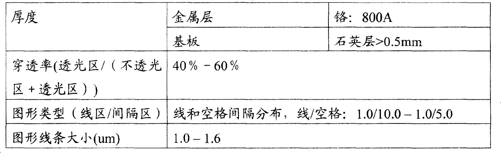
[0013] The present invention provides a sensitive mask, which has some specific technical parameters, as shown in Table 1 below:
[0014] Table 1
[0015]
[0016] A photomask having all the features in Table 1 is the sensitive photomask of the present invention.
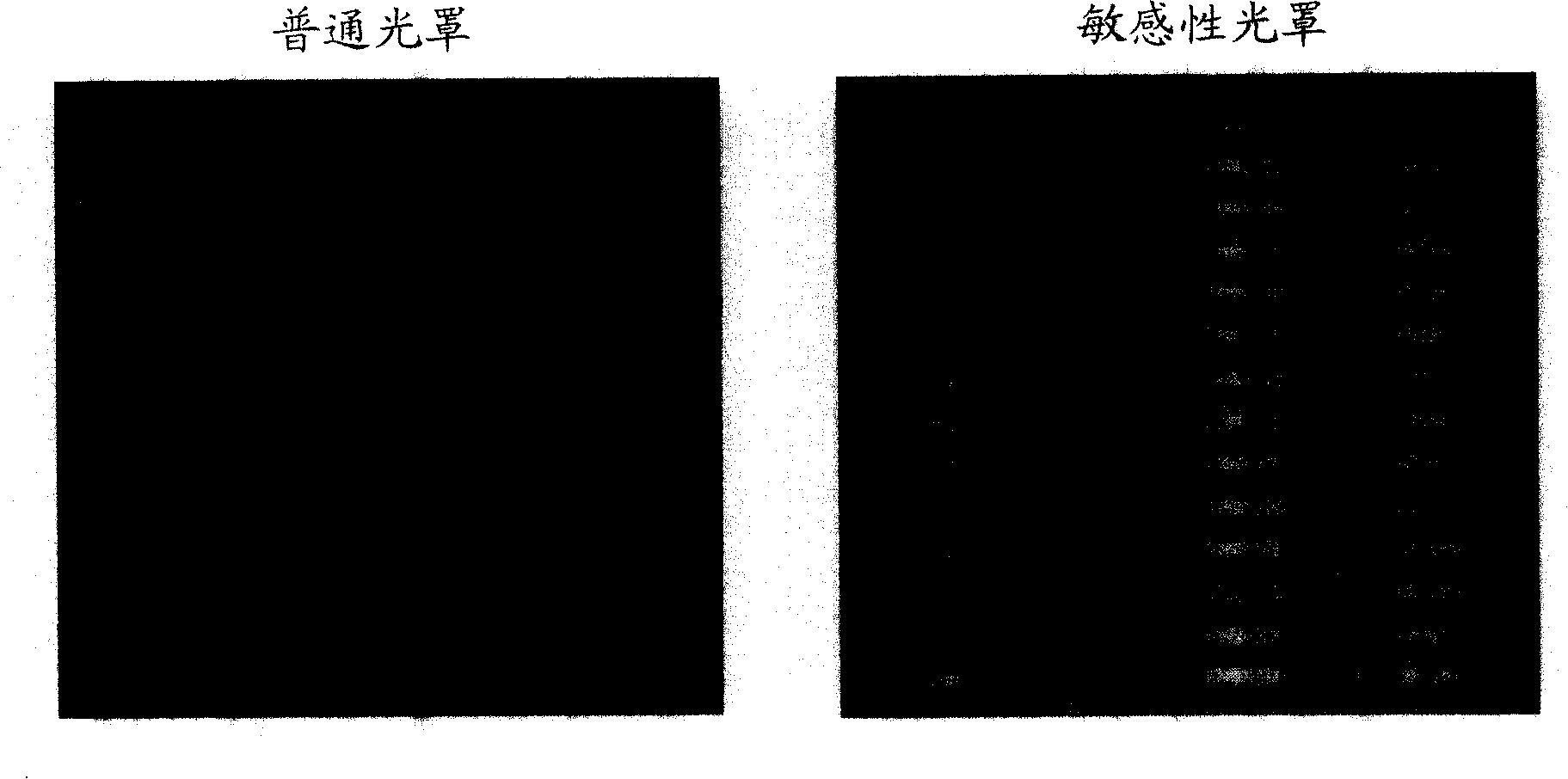
[0017] see figure 1 , the white highlights are the crystals. Experiments have proved that under the same conditions, the sensitive mask is more likely to grow crystals during the exposure process than the common mask.
Login to View More PUM
| Property | Measurement | Unit |
|---|---|---|
| thickness | aaaaa | aaaaa |
| transmittivity | aaaaa | aaaaa |
Abstract
The invention provides a sensitive mask, which is at least composed of a quartz layer and chromium which is covered on the surface of the quartz layer; wherein the thickness of the quartz layer of the mask is larger than 0.5mm, and the thickness of the chromium is 800A. The light transmission rate of the mask ranges from 40 percent to 60 percent. The pattern type of the mask is formed by lines and spaces which are arranged at intervals. The ratio of the lines and the spaces of the pattern of the mask ranges from 1.0 / 10.0 to 1.0 / 5.0. The size of the lines of the pattern of the mask ranges from 1.0um to 1.6um. Compared with the prior art, the sensitive mask of the invention has specific thickness, light transmission rate, pattern type and size of the pattern type; under the same conditions, the sensitive mask can develop a crystal faster than a prior mask, thereby taking remedial measures in the follow-up manufacturing process more earlily.
Description
technical field [0001] The present invention relates to a photomask, in particular to a sensitive photomask. Background technique [0002] During the exposure process, the quality of the photomask affects the quality of the entire pattern formation. In the manufacturing process of the photomask, sulfuric acid, nitric acid and other chemicals are usually involved. Due to the existence of these chemicals, some tiny atoms will be left in the photomask. When the photomask with hidden tiny atoms is illuminated during the exposure process, these tiny atoms will combine with ions in the air to form some crystals, and these crystals will cause dead spots on the exposed wafer. [0003] The current photomask manufacturing process cannot avoid the generation of fine atoms, but if these photomasks with fine atoms are found earlier, remedial measures can be taken in the subsequent manufacturing process. However, the existing technology cannot detect the photomask with fine atoms in time...
Claims
Login to View More Application Information
Patent Timeline
 Patent Type & AuthorityApplications(China)
IPC IPC(8): G03F1/08G03F1/00G03F1/48
Inventor杨金坡张轶楠
OwnerSEMICON MFG INT (SHANGHAI) CORP