Multiple reaction cavity atom layer deposition device and method

An atomic layer deposition, multi-reaction technology, used in coatings, metal material coating processes, gaseous chemical plating, etc., can solve problems such as environmental hidden dangers, waste of reaction sources, prolonged operation time, etc., reaching the dangerous level of environmental damage Lower, less waste, better response control effect

Inactive Publication Date: 2010-06-02
TSINGHUA UNIV
View PDF3 Cites 0 Cited by
  • Summary
  • Abstract
  • Description
  • Claims
  • Application Information

AI Technical Summary

Problems solved by technology

Due to repeated vacuuming, the reaction source will be wasted, the operation time will be prolonged, and it will also bring environmental hazards

Method used


Image

  • Multiple reaction cavity atom layer deposition device and method
  • Multiple reaction cavity atom layer deposition device and method

Examples


Embodiment Construction

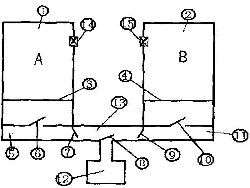
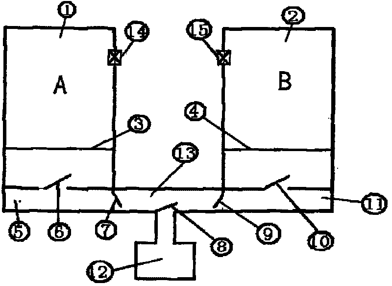
[0029] The invention provides an atomic layer deposition device and method with multiple reaction chambers. The main structure of the device is as figure 1 As shown, in the figure, the A-phase reaction chamber and the B-phase reaction chamber are connected in parallel on a group of vacuum pump groups 12 through a transition chamber 13; the a-reaction chamber 5 at the bottom of the A-phase reaction chamber communicates with the transition chamber 13 through the first channel valve 7; The b reaction chamber 11 of the lower part of the B phase reaction chamber is communicated with the transition chamber 13 through the second channel valve 9, and the a storage chamber 1 and the a partition plate 3 are arranged in the A phase reaction chamber, and the a storage chamber 1 is connected with the first vacuum valve 6 through the first vacuum valve 6. The a reaction chamber 5 of the lower part communicates, and the b storage chamber 2 and the b partition 4 are arranged in the B phase re...


PUM


Abstract

The invention belongs to a multi reaction chamber atomic layer deposition apparatus and a method, and belongs to the field of manufacturing equipment of semiconductors and processing technology. The atomic layer deposition apparatus comprises an A reaction chamber and a B reaction chamber, which are connected with a group of vacuum pumps through a transition chamber, the A reaction chamber and theB reaction chamber are reacted, the A reaction chamber and the B reaction chamber are respectively communicated with the reaction chambers and the transition chamber through channel valves, the reaction chambers are connected with a storeroom through a vacuum valve and a baffle of the storeroom, and an air inlet valve is arranged on the upper portion of the storeroom. The deposition method is that wafers of an integrated circuit are transferred back and forth between the A reaction chamber and the B reaction chamber through the channel valves, when transfers to the A reaction chamber, A phasereaction is produced, when transfers to the B reaction chamber, B phase reaction is produced, the A and the B phase reactions are conducted alternatively, and nanometer-thin layers or compound structure materials with thickness which is demanded by the integrated circuit are grown on each atomic layer of the surface of the wafers. The reaction chamber is less smirched, the deposition quality is improved, the reactant sources amount is saved, the process cost is reduced, and the environment hazard degree is lowest.

Description

technical field [0001] The invention belongs to the technical field of semiconductor manufacturing equipment and processing, and in particular relates to a multi-reaction chamber atomic layer deposition device and method. Background technique [0002] Atomic Layer Deposition (ALD) is a deposition technique for two-phase reaction in a heated reaction chamber. Among them, the first phase reaction is mainly the adsorption process of the reaction gas phase precursor, which will be automatically terminated when the surface is saturated, while the second phase reaction can be generated on the surface of the substrate wafer by introducing another reaction precursor. An atomic layer of a particular material. In this way, it grows up layer by layer until the material deposition reaches the desired thickness. [0003] The materials that can be deposited by ALD technology include: oxides, nitrides, fluorides, metals, carbides, and sulfides, and their nano-thin layers and their compos...

Claims


Application Information

Patent Timeline
Patent Type & Authority Patents(China)
IPC IPC(8): C23C16/44
Inventor 严利人刘志弘刘朋窦维治韩冰
Owner TSINGHUA UNIV
Why Eureka
Try Eureka