A high voltage N-type MOS transistor and the corresponding manufacturing method

A technology of semiconductor tubes and oxides, applied in semiconductor/solid-state device manufacturing, semiconductor devices, electrical components, etc., can solve problems such as incompatibility, achieve good compatibility, improve overall life, and reduce hot carrier injection. Effect

Inactive Publication Date: 2010-06-16
SOUTHEAST UNIV
View PDF5 Cites 0 Cited by
  • Summary
  • Abstract
  • Description
  • Claims
  • Application Information

AI Technical Summary

Problems solved by technology

In some specific processes, the gate oxide layer is also strengthened to reduce the defect density and improve the reliability of the device, such as doping F and Cl in the gate oxide layer or replacing silicon dioxide with silicon nitride, etc. However, this method also has the disadvantage of being incompatible with the current common process.

Method used


Image

  • A high voltage N-type MOS transistor and the corresponding manufacturing method
  • A high voltage N-type MOS transistor and the corresponding manufacturing method

Examples


Embodiment 1

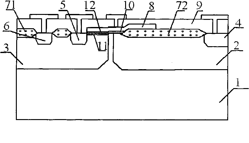
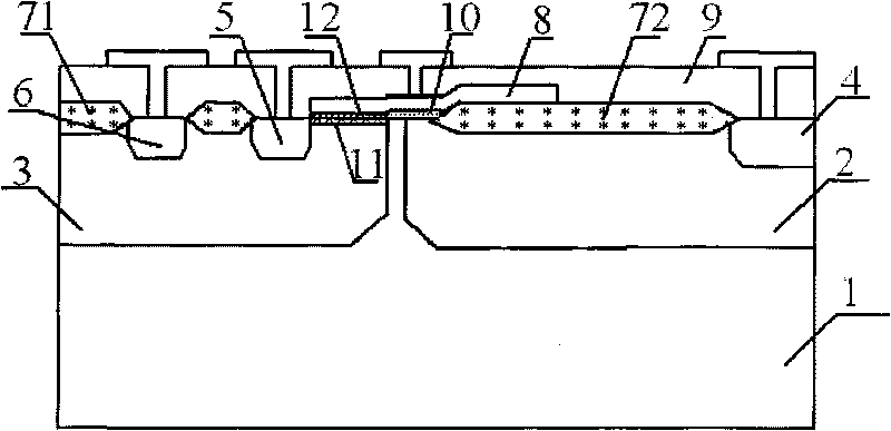
[0014] A high-voltage N-type metal oxide semiconductor tube, comprising a P-type substrate 1, a P-type well 3 and an N-type drift region 2 are arranged on the P-type substrate 1, and a P-type contact hole is arranged on the P-type well 3 6. N-type source 5 and field oxide layer 71, N-type drain 4 and field oxide layer 72 are provided on N-type drift region 2, and P-type well 3, N-type drift region 2 and part of P-type substrate 1 A gate oxide layer is provided above and the gate oxide layer is located between the N-type source 5 and the field oxide layer 72 on the N-type drift region 2. A polysilicon gate 8 is provided on the gate oxide layer and the polysilicon gate 8 extends to the N-type On the field oxide layer 72 on the drift region 2, on the field oxide layer 71 on the P-type well, the P-type contact hole 6, the N-type source 5, the polysilicon gate 8, and the field oxide layer 72 on the N-type drift region (2) And the N-type drain 4 is provided with an oxide layer 9, th...

Embodiment 2

[0016] A method for preparing a high-voltage N-type metal oxide semiconductor tube. First, select a P-type substrate, prepare a P-type well and an N-type drift region on the P-type substrate, and then prepare a field oxide layer, and then perform thick gate oxidation. The growth of the thick gate oxide layer and the etching of the thick gate oxide layer are performed at the same time as the P-type impurity implantation region under the thin gate oxide region, and then a thin gate oxide layer is grown on the P-type impurity implantation region, and then the growth and etching of the polysilicon gate , followed by the source and drain implantation and the substrate contact implantation area, and finally the lead hole, the preparation and passivation treatment of the aluminum lead. The entire process can be realized on the basis of standard epitaxial low-voltage metal-oxide-semiconductor process lines.


PUM


Abstract

The invention discloses a high-voltage N-type metal oxide semiconductor, including a P-type substrate, a P-well drift region and an N-type drift region are arranged on the P-type substrate, a P-type contact hole, an N-type source and a field oxide layer are arranged on the P-well, an N-type drain and the filed oxide layer are arranged on the N-type drift region; the invention is characterized in that the thickness a grid oxide layer part which is positioned above the P-well is smaller than the grid oxide layer part which is positioned above the N-type drift region and a thin grid oxide layer and a thick thin grid oxide layer are respectively formed accordingly, a P-type impurity injection region is arranged in the P-well, and the P-type impurity injection region is positioned below the thin grid oxide layer. The invention further discloses a preparation method of the high-voltage N-type metal oxide semiconductor. The invention has the advantages that the invention can greatly reduce the hot carrier injection phenomenon of a beak region and improve the overall service life of the device; the start voltage, saturated current and other basic electrical characteristics of the device are ensured to be in line with a general structure device; thus the invention has better compatibility.

Description

technical field [0001] The invention relates to a high-voltage N-type metal oxide semiconductor tube and a preparation method thereof, in particular to a high-voltage N-type metal oxide semiconductor tube with high reliability and reduced hot carrier effect and a preparation method thereof. Background technique [0002] In power integrated circuits, high-voltage drive tubes usually work under high-voltage conditions, and the lateral electric field and current density in the device channel are much larger than other devices. Therefore, the hot carrier effect is an inevitable problem in the design of high-voltage drive tubes. The main factor affecting the reliability of the device, especially the current has been in silicon and silicon dioxide (Si, SiO 2 ) Lateral double-diffused metal-oxide-semiconductor transistor (LDMOSFET) with interfacial flow. At present, most of the solutions to the hot carrier effect of metal oxide semiconductor tubes (MOSFET) are aimed at the metal o...

Claims


Application Information

Patent Timeline
Patent Type & Authority Patents(China)
IPC IPC(8): H01L29/78H01L29/423H01L21/336H01L21/28
Inventor 李海松钱钦松孙伟锋易扬波陆生礼时龙兴
Owner SOUTHEAST UNIV
Why Eureka
Try Eureka