Packaging body capable of repeatedly stacking

An encapsulation body and encapsulation colloid technology, applied in semiconductor devices, electric solid state devices, semiconductor/solid state device parts, etc., can solve problems such as cracking, alignment, poor connection, etc.

Inactive Publication Date: 2008-07-16
POWERTECH TECHNOLOGY
View PDF0 Cites 15 Cited by
  • Summary
  • Abstract
  • Description
  • Claims
  • Application Information

AI Technical Summary

Problems solved by technology

Among them, the solder balls 13 of the first package 10 and the solder pads 24 of the second package 20 may have alignment problems.
In addition, during the heating process,

Method used


Image

  • Packaging body capable of repeatedly stacking
  • Packaging body capable of repeatedly stacking
  • Packaging body capable of repeatedly stacking

Examples


Example Embodiment

[0040] The specific implementation of the present invention is described in detail as follows. The preferred embodiment is only an illustration, and is not intended to limit the present invention.
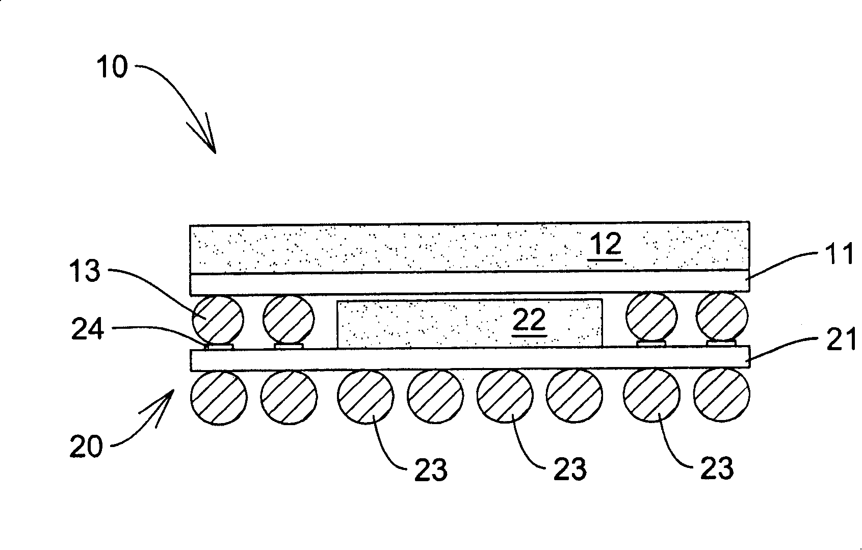
[0041] First, please refer to FIGS. 2A and 2B. FIGS. 2A and 2B show a cross-sectional view of the structure of a first embodiment of a package that can be repeatedly stacked according to the present invention and its stacking diagram. As shown in the figure, the re-stackable package 100 includes a substrate 110, a plurality of first bonding pads, such as bonding pads 120, a chip 130, a plurality of second bonding pads, such as bonding pads 122, and a packaging glue 140 , Which are described below. The substrate 110 has a first surface 112 and a second surface 114, and the second surface 114 is disposed opposite to the first surface 112. In addition, a chip carrier area 116 can be defined on the first surface 112 for subsequent chip placement. A plurality of first bonding pads, such as ...


PUM


Abstract

The invention relates to a package which can be repeatedly piled, comprising a substrate which has a plurality of first welding pads; a chip which is arranged on the substrate and exposes an active surface which is in electric connection with the substrate; a plurality of second welding pads which are arranged on the active surface of the chip; and a package colloid which is arranged on the substrate for covering part of the chip, wherein, the package colloid forms a groove on the active surfaces and exposes second welding pads on the active surface; a plurality of conductive balls are arranged on the second welding pads for electrically connecting first welding pads of another package which can be repeatedly piled. Two packages are piled with the mode of flip chip, the periphery of the substrate is protected by the package colloid, thereby reducing the use of wire leads and improving the warping problem of the two piled packages.

Description

technical field [0001] The invention relates to a stacked chip packaging structure, in particular to a repeatable stackable packaging body stacked in a flip chip manner. Background technique [0002] With the rapid improvement of the functions of products such as computers and network communications, semiconductor technology must have the requirements of diversification, portability, and miniaturization, so that the chip packaging industry must move towards high-precision products such as high power, high density, lightness, thinness, and miniaturization. system development. [0003] With increasing demands for miniaturization and high operating speed, multi-chip packaging structures are becoming more and more common in many electronic devices. Multi-chip configurations minimize system speed constraints by combining two or more chips in a single package. A common multi-chip packaging structure is side-by-side, in which two or more chips are mounted side by side on the same...

Claims


Application Information

Patent Timeline
IPC IPC(8): H01L25/00H01L25/065H01L23/31H01L23/488
CPCH01L2224/32145H01L2224/73207H01L2224/48227H01L2224/32225
Inventor 陈建宏叶昀鑫陈明展
Owner POWERTECH TECHNOLOGY
Why Eureka
Try Eureka