Phase-modulating apparatus

A technology of phase modulation and spatial light modulator, which is applied in nonlinear optics, static indicators, optics, etc., and can solve the problems that the irregularity and inaccuracy of the phase modulation amount cannot be corrected

Active Publication Date: 2008-07-23
HAMAMATSU PHOTONICS KK
View PDF1 Cites 45 Cited by
  • Summary
  • Abstract
  • Description
  • Claims
  • Application Information

AI Technical Summary

Problems solved by technology

Therefore, this method cannot correct the irregularity of the phase modulation amount caused by the voltage-dependent phase modulation characteristic among the pixels
As a result, the method is less accurate when calibrating LCoS SLMs with severe deformations

Method used


Image

  • Phase-modulating apparatus
  • Phase-modulating apparatus
  • Phase-modulating apparatus

Examples


no. 1 approach

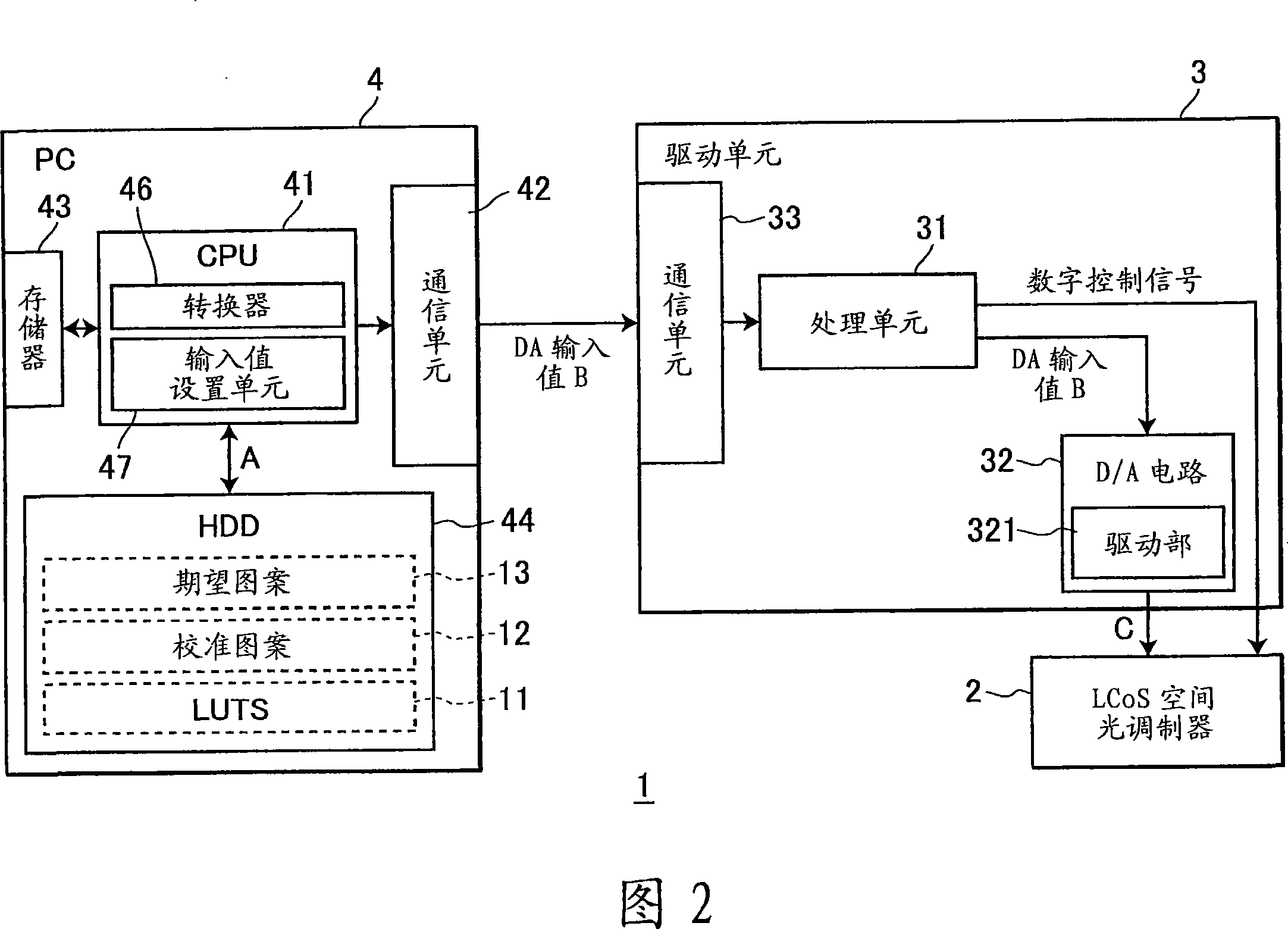
[0057] First, a first embodiment of the present invention will be described with reference to FIGS. 2 to 17(B). As shown in FIG. 2 , the LCoS phase modulator 1 according to the first embodiment includes: an LCoS spatial light modulator 2; a driving unit 3 for applying a voltage to the LCoS spatial light modulator 2; and a control unit 4 for applying a voltage to the LCoS spatial light modulator 2; Data such as control input values ​​described later are sent to the drive unit 3 .

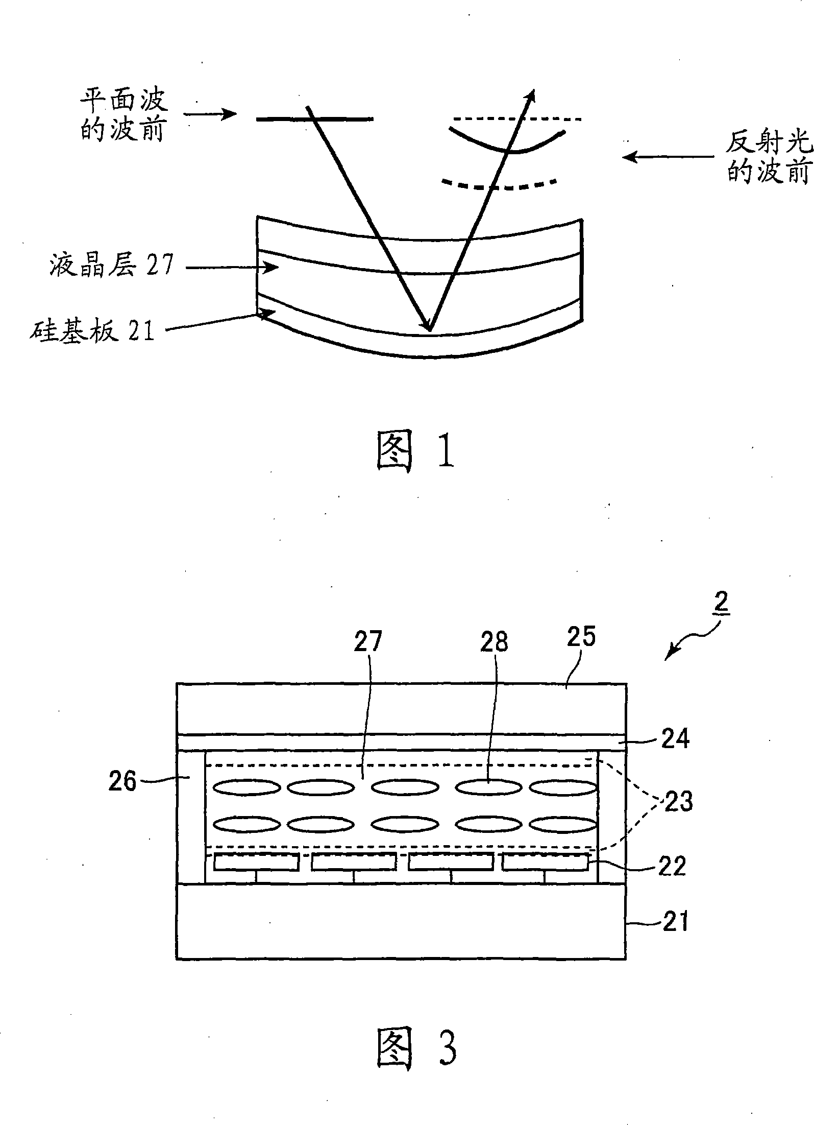
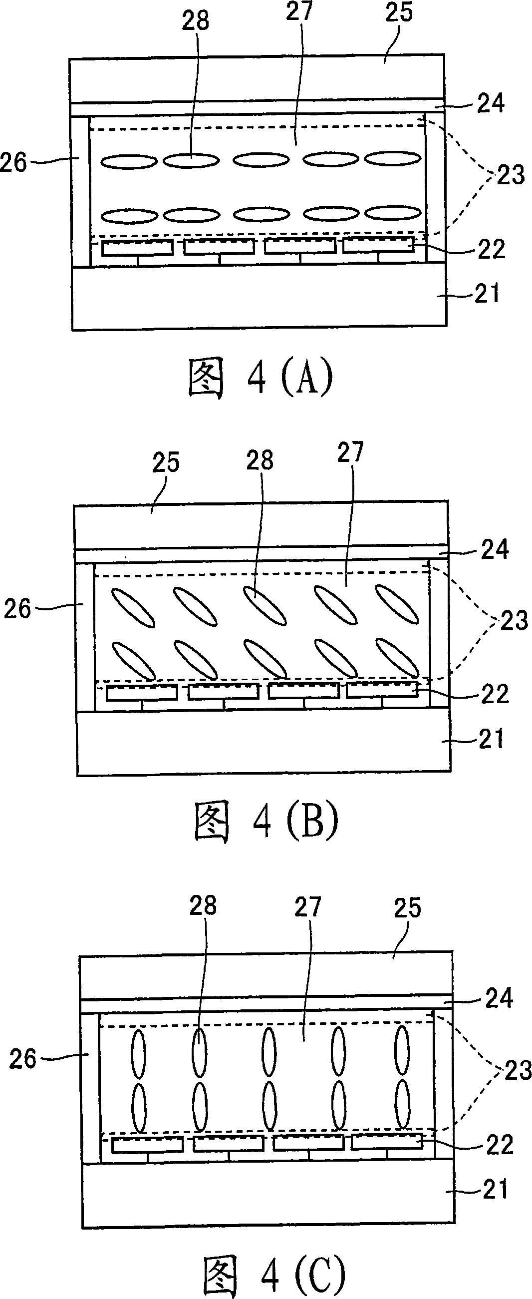
[0058] As shown in FIG. 3 , the LCoS spatial light modulator 2 includes: a silicon substrate 21 , a spacer 26 , and a glass substrate 25 bonded to the silicon substrate 21 through the spacer 26 . A space formed between the silicon substrate 21 and the glass substrate 25 is filled with a liquid crystal layer 27 having liquid crystal molecules 28 . A plurality of pixel electrodes 22 and a circuit (not shown) for controlling voltage applied to the pixel electrodes 22 are formed on the silicon substrate...

no. 2 approach

[0148] Next, a second embodiment of the present invention will be described with reference to FIGS. 22 to 29 . In the first embodiment described above, the LUT 11 is prepared for each pixel to calibrate the voltage-dependent phase modulation characteristic of the pixel. In the second embodiment, a plurality of pixels having similar voltage-dependent phase modulation characteristics are combined into one group, and one LUT 51 is prepared for each group.

[0149] As shown in FIG. 22 , the LCoS phase modulator 500 according to this embodiment includes: an LCoS spatial light modulator 2 , a drive unit 530 for driving the LCoS spatial light modulator 2 with a voltage, and a control unit 4 . Components and components similar to those of the first embodiment described above are denoted by the same reference numerals to avoid duplication of description.

[0150] In the second embodiment, a total of T pixels are divided into r groups based on their voltage-dependent phase modulation c...

no. 8 approach

[0254] It is also possible to replace the D / A circuit 532 with a pulse modulation circuit. With this configuration, the pulse modulation circuit outputs a digital pulse modulation signal for driving the LCoS spatial modulator.

[0255]

[0256] In addition, the approximate polynomial data (coefficient a k(I),g-ave , where 1≦I≦J, and the value is “const”) is stored as a reference data set in the ROM (not shown) of the drive unit 530 instead of the LUT 51 . Similar to the method (S128) of generating the LUT 51 in the second embodiment, according to the number of times of returning to S123, this data is used to obtain equations (18-1) to (18-3). Therefore, the relationship between the control input value A and the DA input value B can be obtained from Equation (18-1) to Equation (18-3). When the phase modulation amount is measured, the LUT processor 536 converts the control input value A into a DA input value B based on the data (S107). Instead of the LUT 51 or the coefficie...


PUM


Abstract

A phase-modulating apparatus includes a spatial light modulator, an input value setting unit, a plurality of sets of reference data, a converting unit, and a driving unit. The input value setting unit sets an input value for each pixel. Each set of reference data corresponds to at least one pixel. The converting unit converts an input value inputted for each pixel to a control value by referencing the corresponding set of reference data. The driving unit converts the control value to a voltage value. The driving unit drives each pixel with a drive voltage corresponding to the voltage value. Each set of reference data correlates a plurality of first values from which input values are taken, and a plurality of second values from which control values are taken to ensure that the relationship between the plurality of first values and phase modulation amounts attained by the corresponding at least one pixel is a prescribed linear relationship.

Description

technical field [0001] The invention relates to a phase modulation device and a method for setting the phase modulation device. Background technique [0002] Spatial light modulators (SLMs) using liquid crystals on silicon (LCoS) are known in the prior art. When a voltage is applied to the pixel electrode, the liquid crystal molecules in the LCoS rotate in the vertical plane of the substrate, thereby adjusting the amount of phase modulation of the incident light. However, since the phase modulation amount changes nonlinearly with respect to the voltage applied to the pixel electrode, a desired phase modulation amount has not yet been obtained. [0003] Figure 1 shows a conceivable LCoS spatial light modulator. Since the LCoS silicon substrate 21 is formed during semiconductor processing, the silicon substrate 21 cannot be made thick, and thus its mechanical strength is low. Therefore, as shown in FIG. 1, stress generated during the process of manufacturing the LCoS elemen...

Claims


Application Information

Patent Timeline
Patent Type & Authority Applications(China)
IPC IPC(8): G02F1/133G02F1/1362G09G3/36
Inventor 松本直也井上卓福智昇央小林祐二原勉
Owner HAMAMATSU PHOTONICS KK
Why Eureka
Try Eureka