Silicon base medium blocking type 1-dimention nano pole structure

A dielectric barrier and nano-electrode technology, applied in the direction of nanostructure manufacturing, nanotechnology, nanotechnology, etc., can solve problems such as deformation and displacement, difficulty in uniform film thickness, and contact, so as to reduce the probability of ignition damage and reduce the electrode Effects of short-circuit problem, stability and life improvement

Inactive Publication Date: 2010-07-21
SHANGHAI JIAOTONG UNIV
View PDF0 Cites 0 Cited by
  • Summary
  • Abstract
  • Description
  • Claims
  • Application Information

AI Technical Summary

Problems solved by technology

[0003] However, the manufacturing process of one-dimensional nanomaterial film is usually difficult to make the film thickness uniform, which cannot be completely avoided in the existing common processes
In this way, it is very difficult to control the electrode gap at the level of a few microns, because under the condition of ensuring the average gap on the entire electrode plane, some local areas are likely to contact the upper and lower electrodes due to uneven film thickness, thus causing a short circuit.
On the other hand, in a one-dimensional nanomaterial film, under a certain loading voltage, the one-dimensional nanomaterial is not completely fixed, but will undergo certain deformation and displacement due to the action of the electric field force. Very common, this phenomenon will also cause contact between the upper and lower electrodes in some localized areas of the membrane, resulting in a short circuit
[0004] After searching the prior art documents, it was found that R B Sadeghian and M Kahrizi published a paper "A method based on A new type of gas ionization sensor with vertical gold nanowires" records a structure of a one-dimensional nano-electrode system, which requires three separate substrates to form the upper and lower electrodes and the isolation layer in between. The manufacturing process is simple stacking. The material and molding process of each substrate make it difficult to realize the electrode structure with an on-chip manufacturing process based on microelectronics processing technology, and it is very difficult to precisely control the gap on the order of several microns, because the thickness of the intermediate layer material is difficult to control. on the order of a few microns

Method used


Image

  • Silicon base medium blocking type 1-dimention nano pole structure
  • Silicon base medium blocking type 1-dimention nano pole structure

Examples


example 1

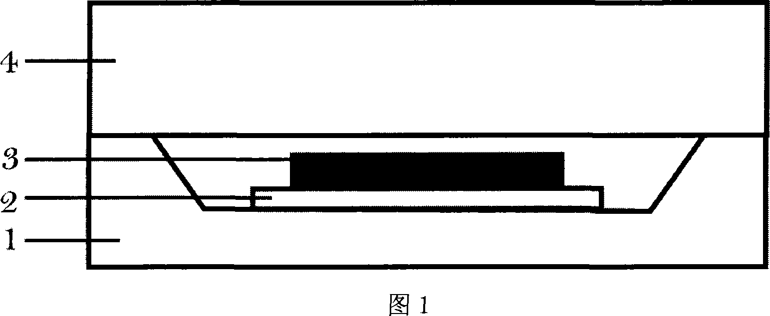
[0017] As shown in Figure 1, this embodiment includes: the electrode structure is formed by bonding two silicon substrates, the upper part and the lower part, and the surface of the lower silicon substrate 1 facing the upper silicon substrate 4 is covered with an insulating layer, and the lower silicon substrate 1 is covered with an insulating layer. Part of the sheet 1 has a pit structure, and a patterned one-dimensional nanomaterial film 3 is arranged in the pit, and a patterned metal conductive layer 2 is arranged on the lower part of the one-dimensional nanomaterial film 3, and the bonded part of the two silicon substrates It is the area around the pit structure of the lower silicon substrate 1, the surface of the upper silicon substrate 4 facing the lower silicon substrate 1 is covered by an insulating layer, and there is an electrode gap between the carbon nanotube film and the upper silicon substrate 4 .

[0018] The one-dimensional nanomaterial film 3, wherein the one-...

example 2

[0025] In this embodiment, the electrode structure is formed by bonding two upper and lower silicon substrates with an area of ​​8 mm × 8 mm. The surface of the lower silicon substrate 1 facing the upper silicon substrate 4 has a silicon dioxide layer with a thickness of 2 μm. Covered by an insulating layer, the central area of ​​the lower silicon substrate 1 has a square groove-shaped pit structure with an area of ​​5mm×8mm, and a square carbon nanotube film with an area of ​​4mm×4mm is arranged in the pit, and the lower part of the carbon nanotube film is arranged There is a Cr / Au metal conductive layer 2 with an area of ​​4.5mm×8mm square and a thickness of 30nm and 270nm respectively. The metal conductive layer 2 is located in the pit of the lower silicon substrate 1 and serves as the conductive connection layer of the carbon nanotube film. The surface of the upper silicon substrate 4 with an area of ​​8 mm × 8 mm facing the lower silicon substrate 1 is covered with a silic...


PUM

PropertyMeasurementUnit
electrical resistivityaaaaaaaaaa
diameteraaaaaaaaaa
thicknessaaaaaaaaaa

Abstract

The invention provides a silicon-based dielectric barrier type one-dimensional nanometer electrode structure, belonging to the micro electric device field. The invention is formed by an upper part silicon-based plate and a lower part silicon-based plate which are bonded, wherein the lower part silicon-based plate is locally provided with a drop-pit structure; the drop-pit is provided inside with a graphical one-dimensional nanometer material film which has the lower part provided with a graphical metal conduction layer. The silicon base dielectric barrier type one-dimensional nanometer electrode structure is applied to electric devices based on gas discharge, which facilitates to the micromation, integration and mass production of the electric devices; moreover, the silicon base dielectric barrier type one-dimensional nanometer electrode structure can avoid the thermal damage of the heat balance plasma to the electrode, which facilitates the improvement the stability and service life of the devices; the dielectric barrier layer can greatly lower the probability of local short circuit, which facilitates the decrease of the clearance between electrodes and ensuring devices work under a lower operating voltage.

Description

technical field [0001] The invention relates to an electrode structure in the technical field of microelectronic devices, in particular to a silicon-based dielectric barrier type one-dimensional nanometer electrode structure. Background technique [0002] Since one-dimensional nanomaterials have tiny diameters on the order of nanometers, if a one-dimensional nanoelectrode material film is used as an electrode material to form a so-called "one-dimensional nanoelectrode system", even if the film thickness is relatively small, it is possible to make the adjacent area of ​​the electrode surface Due to the very large aspect ratio (can be as high as 10 3 above order of magnitude) to produce a significant electric field enhancement effect, so that under the same loading voltage, an electric field with field strength dozens of times higher than that of the parallel plate electrode is established in the local area of ​​the electrode gap and the electrode surface. The one-dimensional...

Claims


Application Information

Patent Timeline
Patent Type & Authority Patents(China)
IPC IPC(8): H01J9/02H01J29/02H01L21/00B82B1/00
Inventor 侯中宇蔡炳初张亚非徐东
Owner SHANGHAI JIAOTONG UNIV
Why Eureka
Try Eureka