Manufacturing method of printed circuit board and printed circuit board

A technology for printed circuit boards and manufacturing methods, which is applied in the directions of printed circuit components, printed circuit secondary processing, and final product manufacturing, and can solve the problems of lamination layer thickness, silk screen solder resist ink side erosion, and lamination layer easy to fall off and other problems, to reduce the probability of falling off problems, reduce the probability of short circuit problems, and avoid the effect of side erosion problems

Pending Publication Date: 2022-08-09
SHENNAN CIRCUITS
View PDF0 Cites 0 Cited by
  • Summary
  • Abstract
  • Description
  • Claims
  • Application Information

AI Technical Summary

Problems solved by technology

[0003] At present, the laminated layer is generally formed by screen-printing solder resist ink on the circuit board or coating plastic encapsulant materials; however, the laminated layer formed by the above method is not only easy to fall off, which is not conducive to high-density wiring, but also The lamination layer is thick, which is not conducive to the miniaturization design of the product; at the same time, the silk screen solder resist ink may cause side erosion problems

Method used


Image

  • Manufacturing method of printed circuit board and printed circuit board
  • Manufacturing method of printed circuit board and printed circuit board
  • Manufacturing method of printed circuit board and printed circuit board

Examples


Embodiment Construction

[0036] The technical solutions in the embodiments of the present application will be clearly and completely described below with reference to the drawings in the embodiments of the present application. Obviously, the described embodiments are only a part of the embodiments of the present application, not all of the embodiments. Based on the embodiments in this application, all other embodiments obtained by those of ordinary skill in the art without creative efforts shall fall within the protection scope of this application.

[0037] The terms "first", "second" and "third" in this application are only used for descriptive purposes, and should not be construed as indicating or implying relative importance or implying the number of indicated technical features. Thus, a feature defined as "first", "second", "third" may expressly or implicitly include at least one of that feature. In the description of the present application, "a plurality of" means at least two, such as two, three...


PUM


Abstract

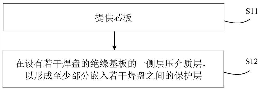
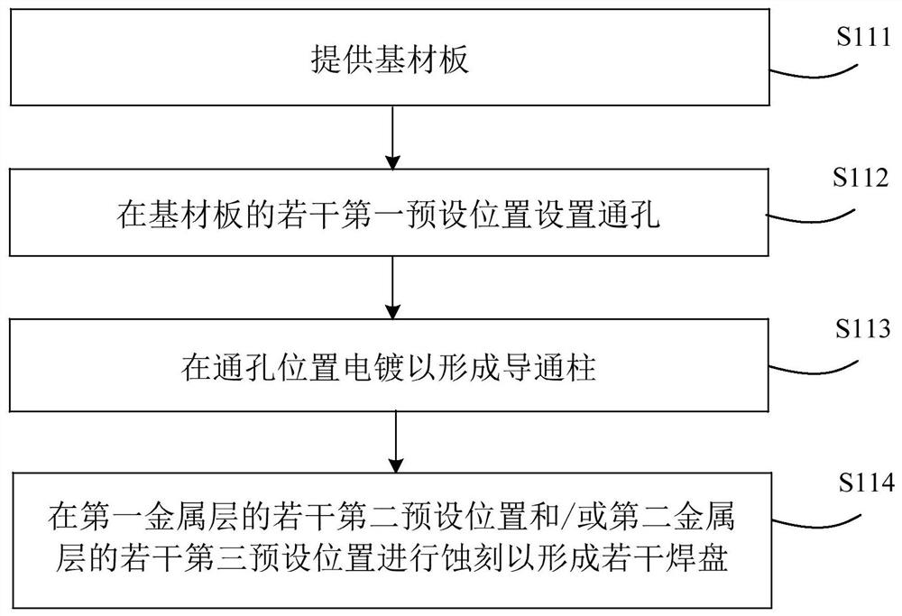
The invention provides a manufacturing method of a printed circuit board and the printed circuit board. The manufacturing method of the printed circuit board comprises the following steps: providing a core board; the core plate comprises an insulating substrate, and a plurality of bonding pads are arranged on a first surface and / or a second surface opposite to the first surface of the insulating substrate; and laminating a dielectric layer on one side of the insulating substrate provided with the plurality of bonding pads to form a lamination layer which is at least partially embedded among the plurality of bonding pads. According to the method, the probability of falling of the lamination layer can be greatly reduced, and the probability of short circuit among the bonding pads during surface mounting of electronic components is further effectively reduced; meanwhile, the thickness of the pressing layer can be controlled within a certain range, the thickness of the pressing layer is effectively reduced, and miniaturization design of products is facilitated.

Description

technical field [0001] The invention relates to the technical field of circuit board processing and manufacturing, in particular to a manufacturing method of a printed circuit board and a printed circuit board. Background technique [0002] In the production process of the circuit board, it is often necessary to set a lamination layer on the surface of the circuit board to protect the circuit layer on the circuit board and avoid short circuits between the pads when mounting electronic components. [0003] At present, the lamination layer is generally formed by silk-screening solder resist ink or coating plastic sealant materials on the circuit board; however, the lamination layer formed by the above method is not only easy to fall off, which is not conducive to high-density wiring, and The lamination layer is thick, which is not conducive to the miniaturized design of the product; at the same time, the silk-screen solder mask ink may cause side etching problems. SUMMARY OF...

Claims


Application Information

Patent Timeline
IPC IPC(8): H05K3/28H05K1/11
CPCH05K3/285H05K1/111H05K3/28H05K1/11
Inventor 唐昌胜
Owner SHENNAN CIRCUITS
Why Eureka
Try Eureka