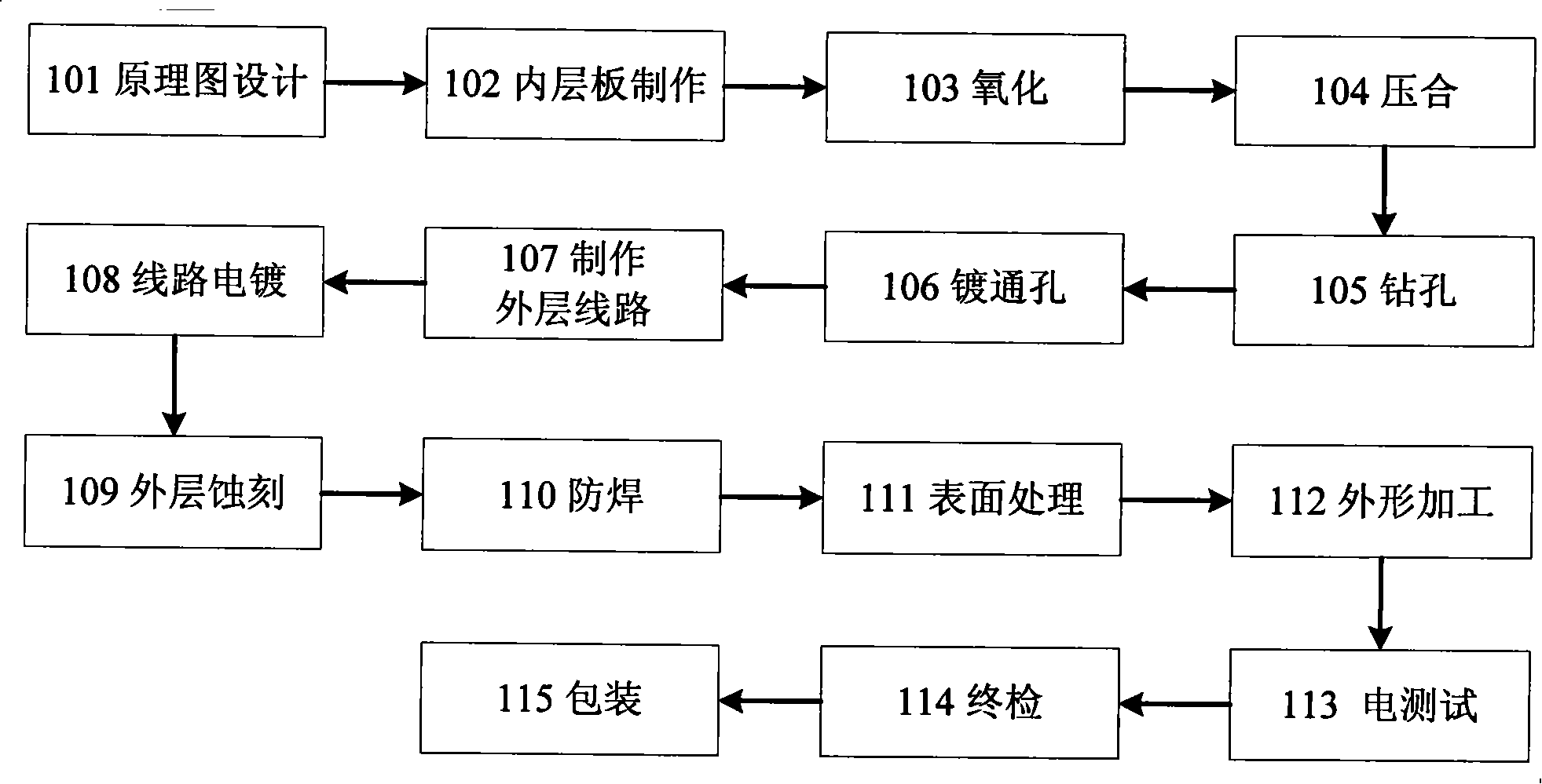
Design producing method of multi-layer printed circuit board
A technology of printed circuit boards and production methods, applied in the direction of multi-layer circuit manufacturing, etc., can solve the problems of unsolved explosion boards, achieve the effect of reducing the probability of explosion, reducing the possibility, and simple and easy operation
- Summary
- Abstract
- Description
- Claims
- Application Information
AI Technical Summary
Problems solved by technology
Method used
Image

Examples
Embodiment Construction
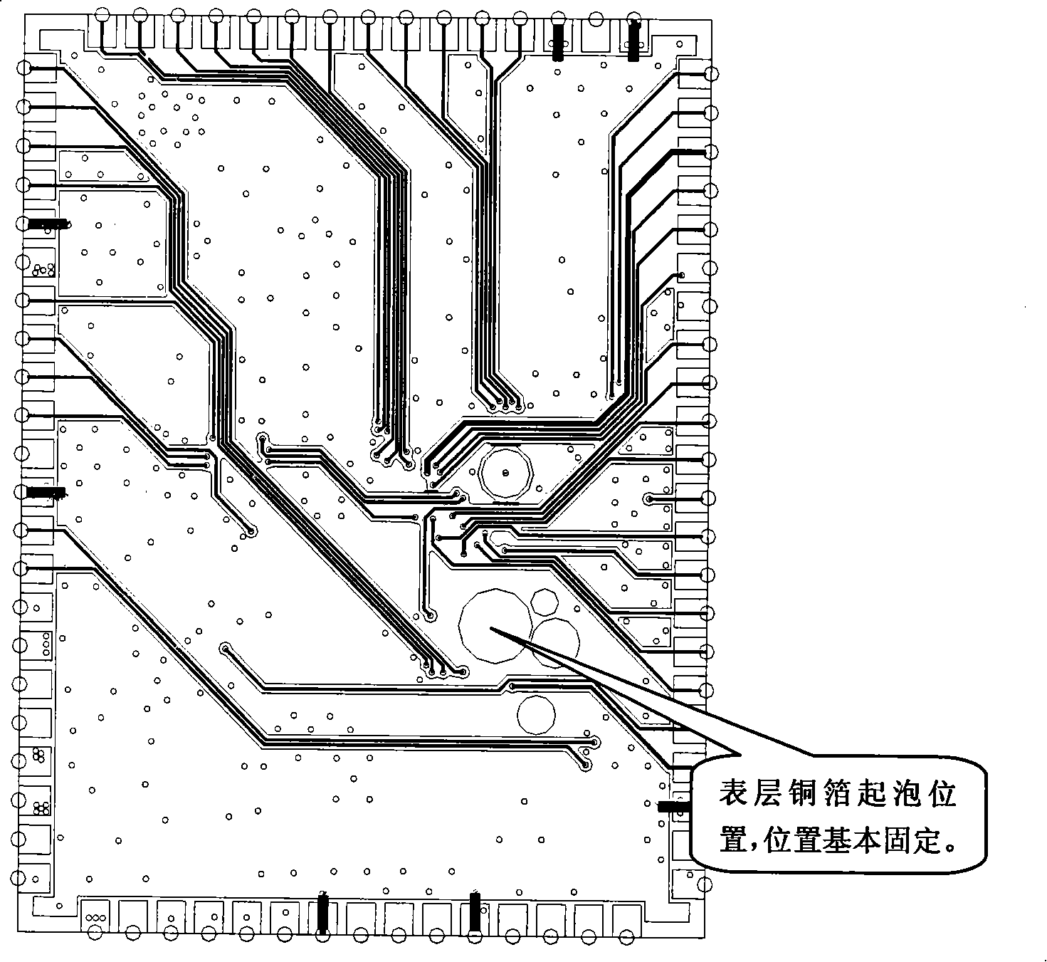
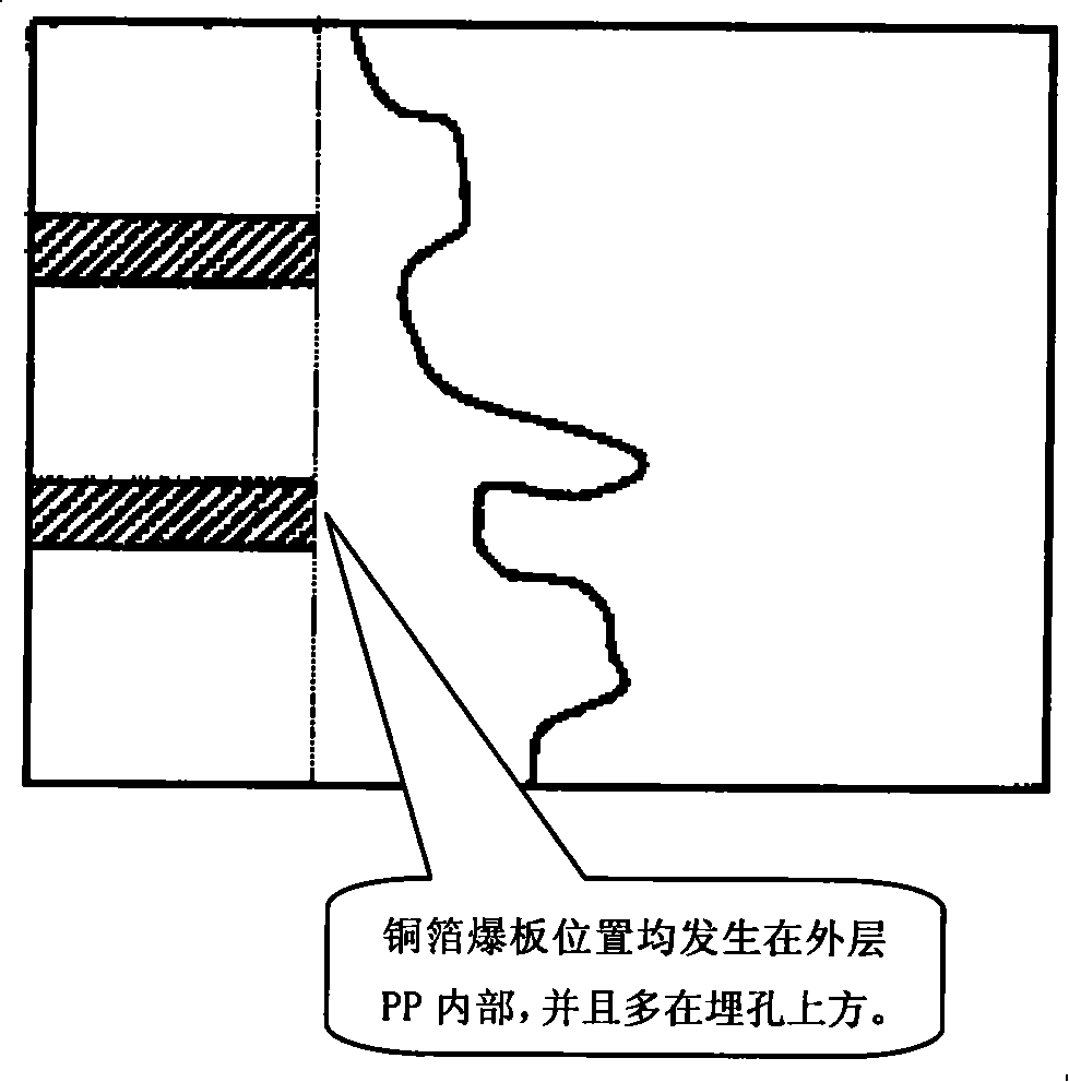
[0026] From the perspective of PCB explosion, moisture absorption is the main reason for PCB delamination. Therefore, the present invention reduces the possibility of PCB board moisture absorption by optimizing the PCB design method and processing flow, thereby reducing the probability of copper foil explosion on the PCB surface. Specifically as follows,
[0027] In the PCB design link:
[0028] ①Using copper foil windows on large areas of copper foil to prevent copper foil from bursting, that is, when laying copper on a large area of PCB surface, properly open some windows to provide a path for the moisture in the board to discharge;
[0029] ② Design heat dissipation ground holes on the large-area copper foil to prevent the surface copper foil from bursting, that is, design some heat dissipation through holes and blind holes, which can effectively increase the heat dissipation area and reduce thermal resistance, and set up conduction holes on the large-area copper foil , ...
PUM
 Abstract
Description
Claims
Application Information
 - R&D
- Intellectual Property
- Life Sciences
- Materials
- Tech Scout
- Unparalleled Data Quality
- Higher Quality Content
- 60% Fewer Hallucinations
Browse by: Latest US Patents, China's latest patents, Technical Efficacy Thesaurus, Application Domain, Technology Topic, Popular Technical Reports.
© 2025 PatSnap. All rights reserved.Legal|Privacy policy|Modern Slavery Act Transparency Statement|Sitemap|About US| Contact US: help@patsnap.com