
Device and method for picking up semiconductor chip

A pick-up device, semiconductor technology, applied in the fields of semiconductor/solid-state device manufacturing, electrical components, circuits, etc., can solve problems such as difficulty in reliably preventing damage, slow pick-up speed, and reduced productivity

Inactive Publication Date: 2008-08-27
SHIBAURA MECHATRONICS CORP
View PDF1 Cites 4 Cited by
  • Summary
  • Abstract
  • Description
  • Claims
  • Application Information

AI Technical Summary

Problems solved by technology

[0006] In order to prevent the breakage of the semiconductor chip due to stress concentration, it can be considered to slow down the speed at which the ejector pin lifts up the semiconductor chip, but if the ejection speed of the ejector pin is slowed down, the pick-up speed will also be slowed down, resulting in a decrease in productivity, or Sometimes even if the jacking speed is slowed down, it is difficult to reliably prevent the damage when the semiconductor chip is thin

Method used


Image

  • Device and method for picking up semiconductor chip
  • Device and method for picking up semiconductor chip
  • Device and method for picking up semiconductor chip

Examples


Embodiment Construction

[0031] Hereinafter, specific embodiments of the present invention will be described with reference to the drawings.

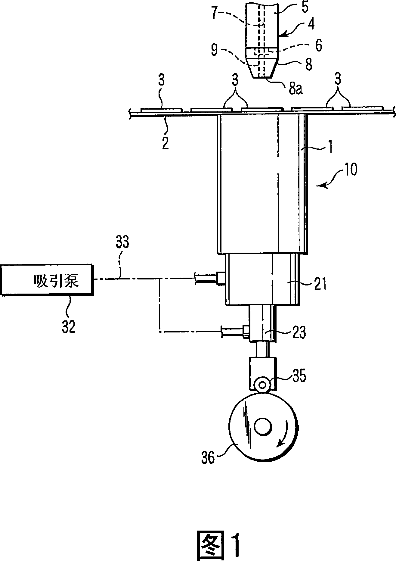
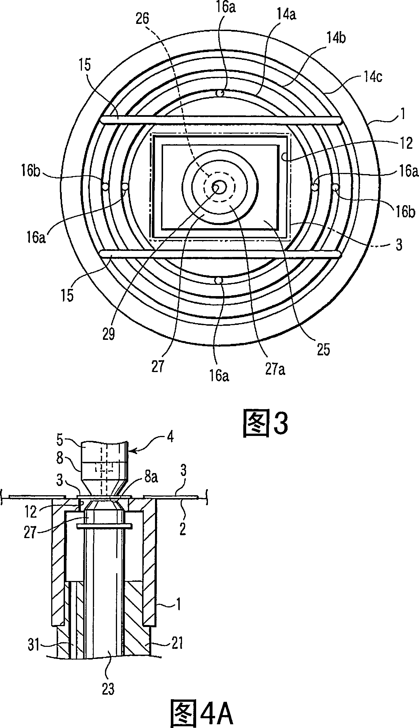
[0032] 1 to 5 show a first embodiment of the present invention. The pickup device shown in FIG. 1 has a support unit 10 . This support unit 10 is provided opposite to the lower surface side of the adhesive sheet 2 tensioned on the unillustrated wafer ring, and is supported along the Z direction by an unillustrated Z driving source as will be described later. The supporting unit 10 is driven between a position where the upper surface of the body 1 is in contact with the adhesive sheet 2 and a position where it is separated from the adhesive sheet 2 .

[0033] On the upper surface of the above-mentioned adhesive sheet 2, a plurality of semiconductor chips 3 divided into small quadrangular blocks are pasted. The wafer ring is driven in the horizontal direction by X and Y drive sources (not shown).

[0034] Accordingly, the semiconductor chip 3 attached to the a...


PUM


Abstract

A device for picking up a semiconductor chip stuck on a tacky adhesive sheet. The device comprises a backup body (1) having an upper surface formed on the sucking surface of the tacky adhesive sheet (2) holdingly sucking the peripheral portion of the semiconductor chip (3) to be picked up, a push-up shaft (23) vertically drivingly installed in the backup body and having a lower suction nozzle body (27) pressing the portion of the tacky adhesive sheet where the semiconductor chip to be picked up is stuck to push up the semiconductor chip from the upper surface of the backup body, and a suction nozzle body (4) suckingly holding the upper surface of the semiconductor chip to be picked up to pick up the semiconductor chip pushed up by the push-up shaft from the tacky adhesive sheet.

Description

technical field [0001] The present invention relates to a pick-up device and a pick-up method for picking up a semiconductor chip stuck on an adhesive sheet. technical background [0002] Semiconductor chips cut into small squares from a semiconductor wafer are attached to an adhesive sheet, and when the semiconductor chip is bonded to a substrate, the semiconductor chips are picked up one by one from the adhesive sheet by a suction nozzle. [0003] When picking up a semiconductor chip from an adhesive sheet, as shown in Patent Document 1, the following method has been conventionally adopted: the peripheral portion of the above-mentioned semiconductor chip on which the adhesive sheet of the semiconductor chip picked up by the suction nozzle is attached to the upper surface of the support The semiconductor chip is sucked and held, and the semiconductor chip is picked up by the suction nozzle while separating the semiconductor chip from the adhesive sheet by pushing up the sem...

Claims


Application Information

Patent Timeline
Patent Type & Authority Applications(China)
IPC IPC(8): H01L21/67H01L21/52
CPCH01L21/67092H05K13/0408
Inventor 太田诚小西宣明岩城泰雄志贺康一
Owner SHIBAURA MECHATRONICS CORP
Learn More