Microstructure appearance test method based on infrared white light interference technique

A technology of white light interference and testing method, which is applied to measurement devices, optical devices, instruments, etc., can solve the problem of inability to measure the sidewall topography of deep trench structures, and achieve the effect of wide application fields

Inactive Publication Date: 2008-09-17
ZHONGBEI UNIV
View PDF0 Cites 31 Cited by
  • Summary
  • Abstract
  • Description
  • Claims
  • Application Information

AI Technical Summary

Problems solved by technology

[0006] In order to solve the problem that the existing testing technology cannot measure the sidewall morphology of the deep groove structure in the MEMS device, the present invention provides a microstructure morphology testing method based on infrared white light interference technology

Method used


Image

  • Microstructure appearance test method based on infrared white light interference technique
  • Microstructure appearance test method based on infrared white light interference technique

Examples


Embodiment Construction

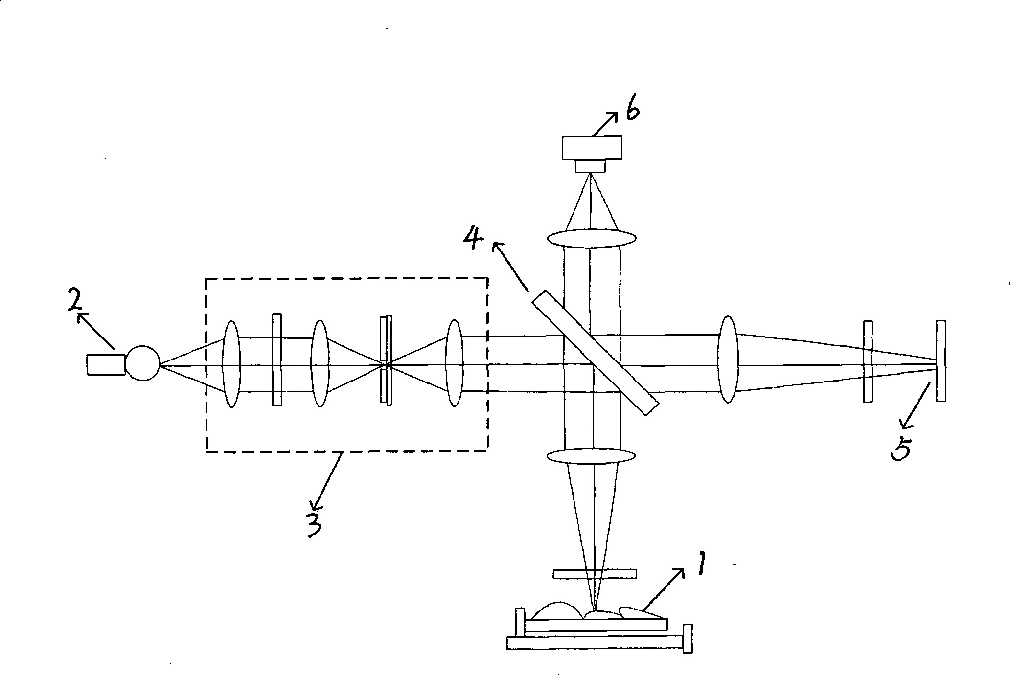
[0016] The microstructure morphology testing method based on infrared white light interference technology is realized in the following steps:

[0017] 1), on the basis of not damaging the surface morphology of the sidewall to be tested in the deep groove structure of the device under test 1, a non-destructive treatment is performed on the sidewall to be tested to prevent infrared transmission;

[0018] 2), (such as figure 1 As shown) the infrared light source 2 is used as the measurement light source. The infrared light emitted by the infrared light source 2 is adjusted by the lens group 3 to become a parallel beam. The parallel beam is divided into a reference beam and a detection beam by the beam splitter 4. The detection beam penetrates the deep groove structure The side wall to be measured is coherently superimposed with the reference beam reflected by the reference mirror 5 after being reflected by the side wall and the non-destructively processed interface, forming a lig...


PUM


Abstract

The invention relates to the micro appearance test of a micro electro-mechanical MEMS component, concretely a microstructure appearance test method based on a white infrared light interference technology, which solves the problem existing in the prior art that the sidewall appearance of the deep trench structure of the MEMS component is unable to be surveyed, realized by the following steps: 1) the lossless processing of the impediment infrared transmission for the testing sidewall surface is carried out; 2) the infrared source is taken as the survey photo source, the infrared light is adjusted to be the parallel light when passing through a lenses group, is divided into a reference beam and a examination light beam by a dispersion component, the examination light beam transmits the sidewall of the deep trench structure, after reflected by the interface of the sidewall and the lossless processing, is carried on coherent superposition with the reference beam reflected by a reference mirror, forms a interference fringe pattern; 3) the interference fringe pattern is transmitted to the computer after passing through an optical lens, the CCD image sensor, so that the three dimensional appearance chart of the sidewall measured is obtained by analyzing and processing. The invention overcomes the shortcoming existing in the prior art that the deep trench structure surveying is unable to be realized and the application domain is wild.

Description

technical field [0001] The invention relates to micro-morphology testing of micro-electromechanical MEMS devices, in particular to a micro-structure topography testing method based on infrared white light interference technology for testing the topography of trench sidewalls in silicon MEMS devices, especially for high depth and width than the deep trench structure. Background technique [0002] With the development of micro-electromechanical systems (MEMS), the requirements for microstructures are getting higher and higher. For the current MEMS high-aspect-ratio microstructures (that is, high-aspect-ratio deep trench structures), such as: using sidewall capacitors The sampling structure and the comb structure of the resonant gyroscope and the roughness of the side wall directly affect the performance of the micromechanical device, such as: driving force, operating frequency range, sensitivity and displacement, etc.; now the width of the MEMS high aspect ratio microstructure...

Claims


Application Information

Patent Timeline
Patent Type & Authority Applications(China)
IPC IPC(8): G01B11/24G01B11/30
Inventor 薛晨阳张文栋熊继军刘俊刘文怡李明魏天杰
Owner ZHONGBEI UNIV
Why Eureka
Try Eureka