Equipment for soldering and planting ball as well as acquisition apparatus

A solder ball and ball planting technology, which is applied in the direction of welding equipment, tin feeding equipment, metal processing equipment, etc., can solve the problems of process cost increase and process cost increase, and achieve the effect of low cost and saving process equipment cost

Active Publication Date: 2008-10-01
SILICONWARE PRECISION IND CO LTD
View PDF9 Cites 11 Cited by
  • Summary
  • Abstract
  • Description
  • Claims
  • Application Information

AI Technical Summary

Problems solved by technology

[0005] However, in the actual process, the problem that is often faced is that, according to the solder ball layout of different types of substrates, it is necessary to change and provide correspondingly different types of solder ball picking devices
Furthermore, due to the continuous improvement of products in the industry, the requirements for the number of I / Os are increasing, so the solder balls and their spacing on the back of the substrate are getting smaller and smaller, so the accuracy requirements of related ball placement equipment are also getting higher and higher. This leads to an increase in process cost, especially for the solder ball pick-up device, because it needs to use precision machining, resulting in a substantial increase in process cost

Method used


Image

  • Equipment for soldering and planting ball as well as acquisition apparatus
  • Equipment for soldering and planting ball as well as acquisition apparatus
  • Equipment for soldering and planting ball as well as acquisition apparatus

Examples


Embodiment Construction

[0058] The implementation of the present invention is described below through specific examples. Those skilled in the art can easily understand other advantages and effects of the present invention from the content disclosed in this specification.

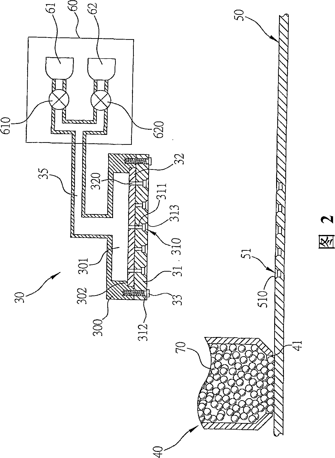
[0059] Please refer to FIG. 2 , which shows the solder ball planting equipment of the present invention, which includes a solder ball setting device 50 , a solder ball storage device 40 , and a solder ball picking device 30 .

[0060]The solder ball holder 50 has a plurality of accommodating holes 51 for accommodating the solder balls 70 disposed on a surface, and each accommodating hole 51 has an oblique section 510 of the accommodating hole surrounding the periphery of the accommodating hole 51, When the solder ball 70 is placed in the accommodating hole 51 , it will not be too tight to take out the solder ball 70 smoothly.

[0061] The solder ball storage device 40 is set close to the surface of the solder ball holder 50 with th...


PUM


Abstract

A solder ball mounting ball apparatus and collecting device thereof are disclosed, the solder ball mounting ball apparatus comprises a solder ball containing instrument whose surface is provided with a plurality of containing holes; a solder ball storing instrument which is used for storing a plurality of solder balls, provided above the solder ball containing instrument in a movable manner of being parallel to the surface direction of the solder ball containing instrument and installed with a supply hole corresponding to the surface of the solder ball containing instrument; and a solder ball collecting device which is provided above the solder ball containing instrument in a movable manner; the solder ball collecting device includes a main body and a first, and a first and second templates provided at one end of the main body in the detachable manner, the main body includes a containing chamber, the first template includes a plurality of a first guide-through holes arrayed in a manner of full matrix and perforated the first template, the second template includes a plurality of a second guide-through holes; and part of the first guide-through holes in the first template is communicated with the second guide-through holes at the corresponding position in the second template, wherein on account of the fact that diverse solder ball distributions are able to vary the disposal locations and quantity of the second guide-through holes in the second template, the cost of process apparatus is saved.

Description

technical field [0001] The invention relates to a semiconductor device, in particular to a solder ball planting device and a picking device thereof. Background technique [0002] Ball Grid Array (BGA) is an advanced semiconductor chip packaging technology, which is characterized in that a substrate is used to place a semiconductor chip, and a plurality of solder balls arranged in a grid array are implanted on the back of the substrate ( Solder Ball), so that more input / output connection terminals (I / O Connection) can be accommodated on the semiconductor chip carrier of the same unit area to meet the needs of highly integrated semiconductor chips, so that these solder balls will The entire packaging unit is soldered and electrically connected to an external printed circuit board. [0003] Such as figure 1 As shown, it is a solder ball planting equipment disclosed in US Patent No. 6,533,159B1 for ball grid array (Ball Grid Array) packaging, which includes a solder ball pick-...

Claims


Application Information

Patent Timeline
Patent Type & Authority Applications(China)
IPC IPC(8): H01L21/48H01L21/60H05K3/34H05K13/04B23K3/06B23K101/40B23K101/42
Inventor 王维宾李德浩王兴召郑坤一黄熴铭
Owner SILICONWARE PRECISION IND CO LTD
Why Eureka
Try Eureka