Organic light emitting display

一种发光显示器、有机的技术,应用在静态指示器、电致发光光源、仪器等方向,能够解决产品可靠性降低、检测到等问题,达到高可靠性、降低模块工艺成本的效果

Inactive Publication Date: 2008-10-08
SAMSUNG DISPLAY CO LTD
View PDF1 Cites 27 Cited by
  • Summary
  • Abstract
  • Description
  • Claims
  • Application Information

AI Technical Summary

Problems solved by technology

However, additional module process operation costs for defective panels required for shorting
When the full inspection is not performed during the module process, since a longitudinal short cannot be detected as a defect during the manufacturing process, the reliability of the product is lowered so that the defect is discovered by the end user of the product

Method used


Image

  • Organic light emitting display
  • Organic light emitting display
  • Organic light emitting display

Examples


Embodiment Construction

[0045] Hereinafter, exemplary embodiments of the present invention will be described in detail with reference to the accompanying drawings.

[0046] It should be understood that an electrical connection between a certain element and another element includes a direct electrical connection between them and an indirect electrical connection between them through an intervening element.

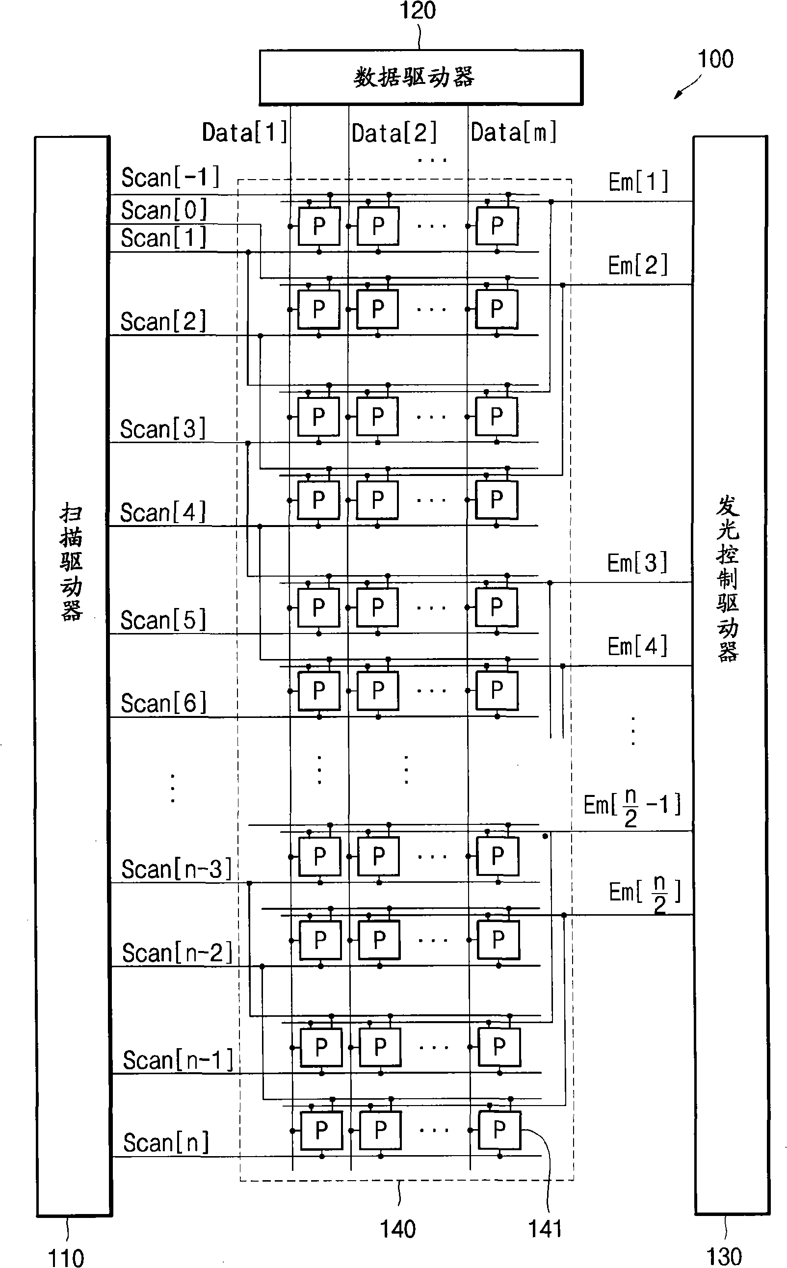
[0047] figure 1 A schematic block diagram of an organic light emitting display according to an exemplary embodiment of the present invention is shown.

[0048] Such as figure 1 As shown in , an organic light emitting display 100 in an exemplary embodiment includes a scan driver 110 , a data driver 120 , an emission control driver 130 and an organic light emitting display panel (hereinafter, referred to as a “panel”) 140 .

[0049] The scan driver 110 may sequentially provide scan signals to the panel 140 through a plurality of scan lines (Scan[−1], Scan[0], Scan[1], Scan[2], . . . , Scan[n]).

...


PUM


Abstract

An organic light emitting display includes: a first shift register which is electrically coupled with a first clock line, a second inverted clock line, and an initial drive line; a first NAND gate which is electrically coupled with the initial drive line, a first light emitting control line which is an output line of the first shift register, and a third clock line; a second NAND gate which is electrically coupled with the initial drive line, the first light emitting control line, and a fourth clock line; a first pixel part which is electrically coupled with a first scan line which is an output line of the first NAND gate; a second pixel part which is electrically coupled with a second scan line which is an output line of the second NAND gate; a third pixel part which is electrically coupled with the first scan line; and a fourth pixel part which is electrically coupled with the second scan line.

Description

[0001] This application claims priority from Korean Patent Application No. 10-2007-0034285 filed on Apr. 6, 2007, the entire contents of which are hereby incorporated by reference. technical field [0002] The invention relates to an organic light emitting display. Background technique [0003] An organic light emitting display is a display that emits light by electrically exciting fluorescent or phosphorescent compounds and can display images by driving N×M organic light emitting diodes. An OLED consists of an anode (ITO), an organic thin film, and a cathode (metal). The organic thin film is formed of a multilayer structure including an emission layer EML that emits light when electrons and holes recombine, an electron transport layer ETL that transports electrons, and a hole transport layer HTL that transports holes. The organic thin film may also include an electron injection layer EIL that injects electrons and a hole injection layer HIL that injects holes. [0004] As...

Claims


Application Information

Patent Timeline
Patent Type & Authority Applications(China)
IPC IPC(8): G09G3/30G09G3/32G11C19/28
CPCG09G3/006G09G3/3233G09G3/3266G09G2300/0819G09G2300/0852G09G2300/0861G09G2310/0224G09G2310/0286G11C19/00G11C19/28H05B33/02
Inventor 金钟允
Owner SAMSUNG DISPLAY CO LTD
Why Eureka
Try Eureka