
Patsnap Eureka
For R&D, Patsnap Eureka makes reading and utilizing patents & technical documents easy.
Patsnap Eureka AIR
Designed for self-driven R&D workflows. Generate viable solutions, solve complex R&D challenges, empower your innovation with AI.

Patsnap Eureka Materials
Designed for material experts only. Revolutionize your material R&D, from search, analyze, to developing new materials.

TechResearch
Generate reliable direction feasibility study reports for your R&D in just a few steps.

TechSeek
Discover and master advanced knowledge NOW. Basics, ideas, possibilities, all at once.

TechMind
As an expert in R&D Theories, TechMind can generates customized viable solutions instantly.

TechRisk
Analyze your overall solution with one click, know your potential R&D risks in advance.

TechMonitor
Get weekly tech updates, stay abreast of the latest tech innovations and key insights.
Method for preparing power MOS tube capable of improving grid oxic horizon homogeneity
A gate oxide, MOS tube technology, applied in semiconductor/solid-state device manufacturing, electrical components, circuits, etc., can solve the problems of large leakage current and easy breakdown of power MOS tube 1, so as to avoid leakage or breakdown. , the effect of improving uniformity
- Summary
- Abstract
- Description
- Claims
- Application Information
AI Technical Summary
Problems solved by technology
Method used
Image

Examples
Embodiment Construction
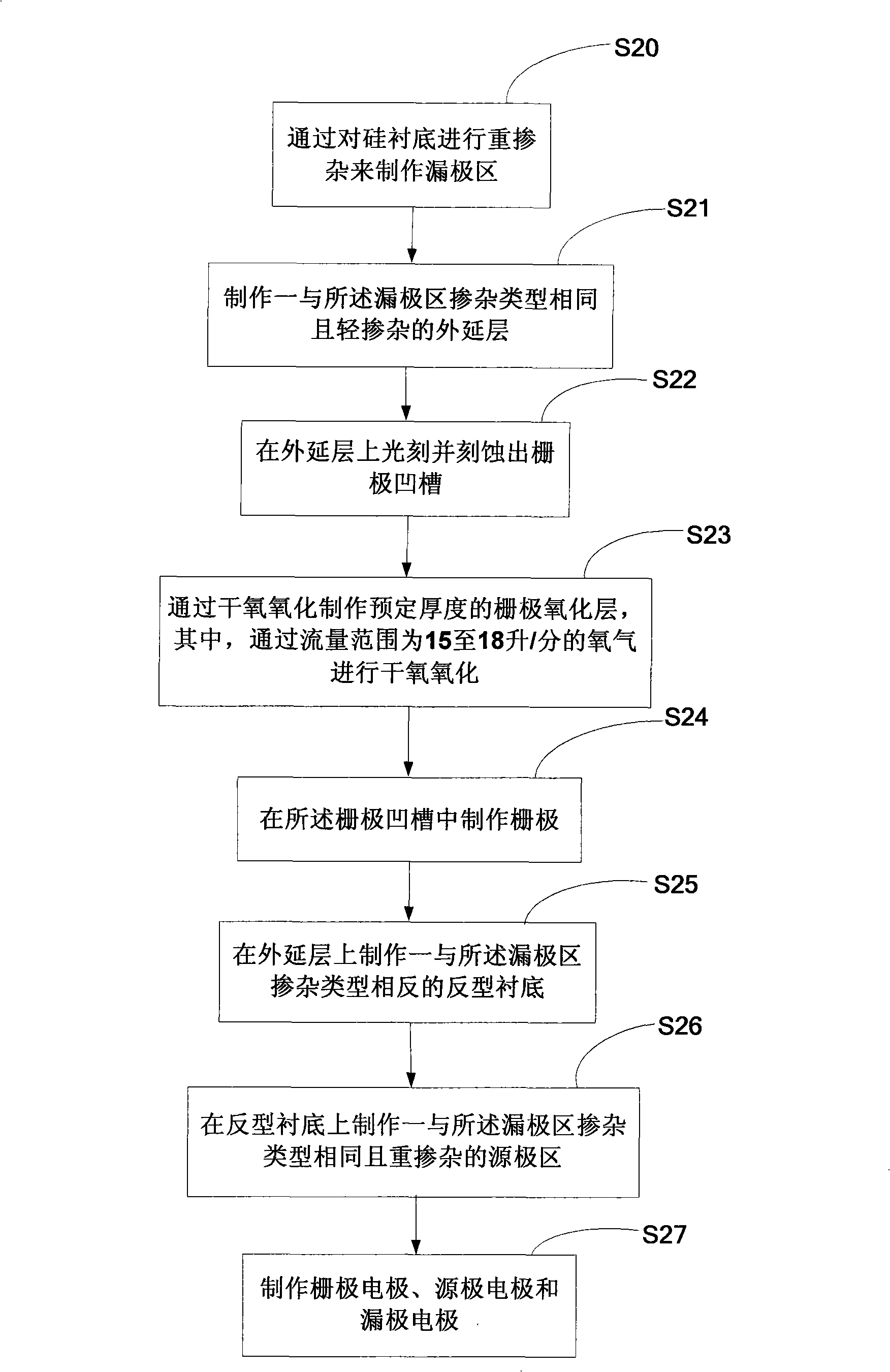
[0024] The fabrication method of the power MOS transistor capable of improving the uniformity of the gate oxide layer of the present invention will be further described in detail below.
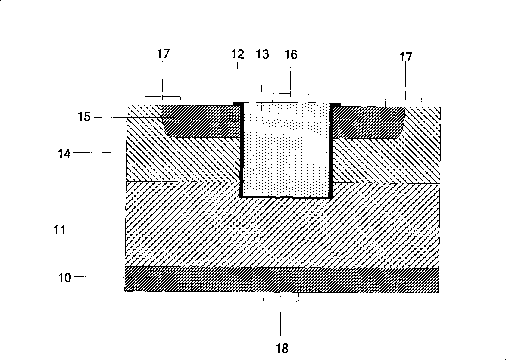
[0025] The power MOS transistor that can improve the uniformity of the gate oxide layer of the present invention is made on a silicon substrate, see figure 2 , the manufacturing method of the power MOS transistor that can improve the uniformity of the gate oxide layer of the present invention firstly performs step S20, and makes the drain region by heavily doping the silicon substrate, wherein, when making the N-channel power MOS transistor N-type heavy doping is carried out on the silicon substrate, and P-type heavy doping is carried out on the silicon substrate when making a P-channel power MOS transistor. In this embodiment, the fabrication of an N-channel power MOS transistor is taken as an example for illustration, so the silicon substrate is heavily doped with N-type.
[0026] see i...
PUM
 Abstract
Description
Claims
Application Information
 - R&D Engineer
- R&D Manager
- IP Professional
- Industry Leading Data Capabilities
- Powerful AI technology
- Patent DNA Extraction
Browse by: Latest US Patents, China's latest patents, Technical Efficacy Thesaurus, Application Domain, Technology Topic, Popular Technical Reports.
© 2024 PatSnap. All rights reserved.Legal|Privacy policy|Modern Slavery Act Transparency Statement|Sitemap|About US| Contact US: help@patsnap.com