
Wafer quality analysis method and device

A quality analysis and wafer technology, applied in the direction of semiconductor/solid-state device testing/measurement, etc., can solve the problems of unstable wafer quality analysis results, subjective wafer quality analysis, etc., and achieve significant failure distribution types and short quality analysis time. , the process of determining the fast effect

Inactive Publication Date: 2008-10-22
SEMICON MFG INT (SHANGHAI) CORP
View PDF1 Cites 10 Cited by
  • Summary
  • Abstract
  • Description
  • Claims
  • Application Information

AI Technical Summary

Problems solved by technology

[0005] The problem solved by the present invention is that wafer quality analysis in the prior art is relatively subjective, resulting in unstable wafer quality analysis results

Method used


Image

  • Wafer quality analysis method and device
  • Wafer quality analysis method and device
  • Wafer quality analysis method and device

Examples


Embodiment Construction

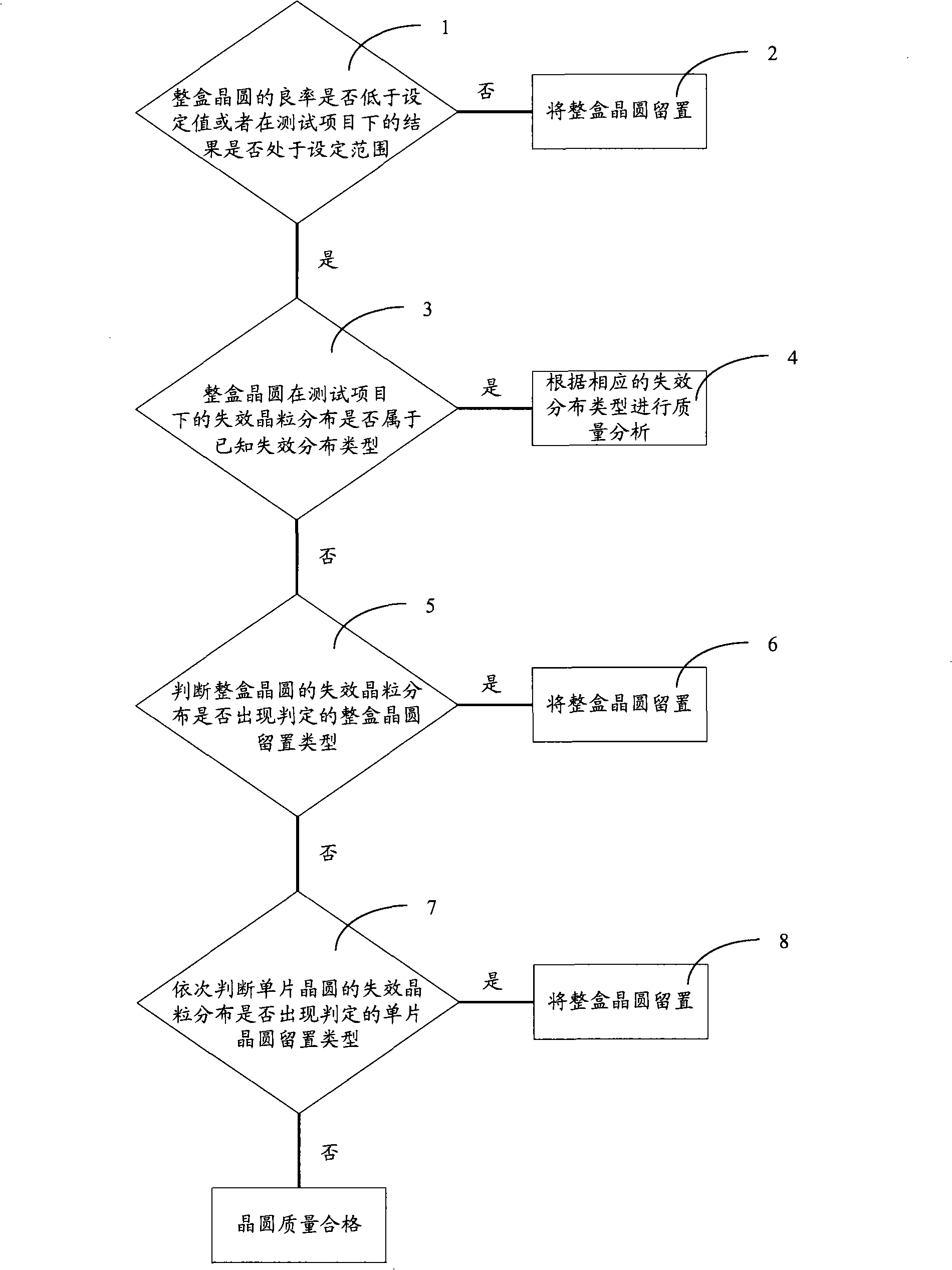
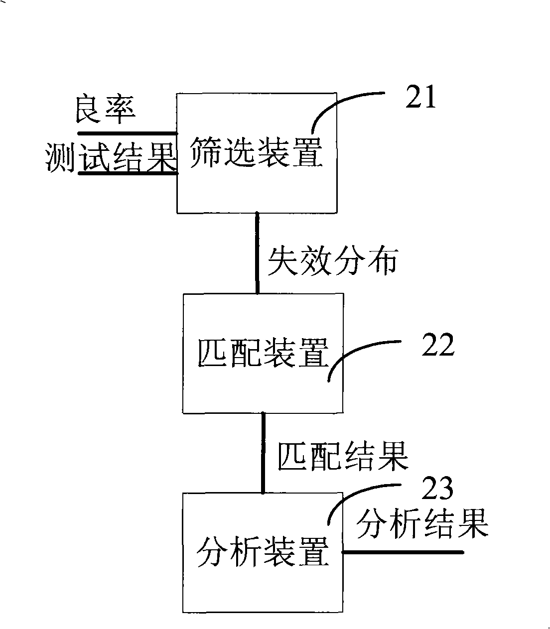
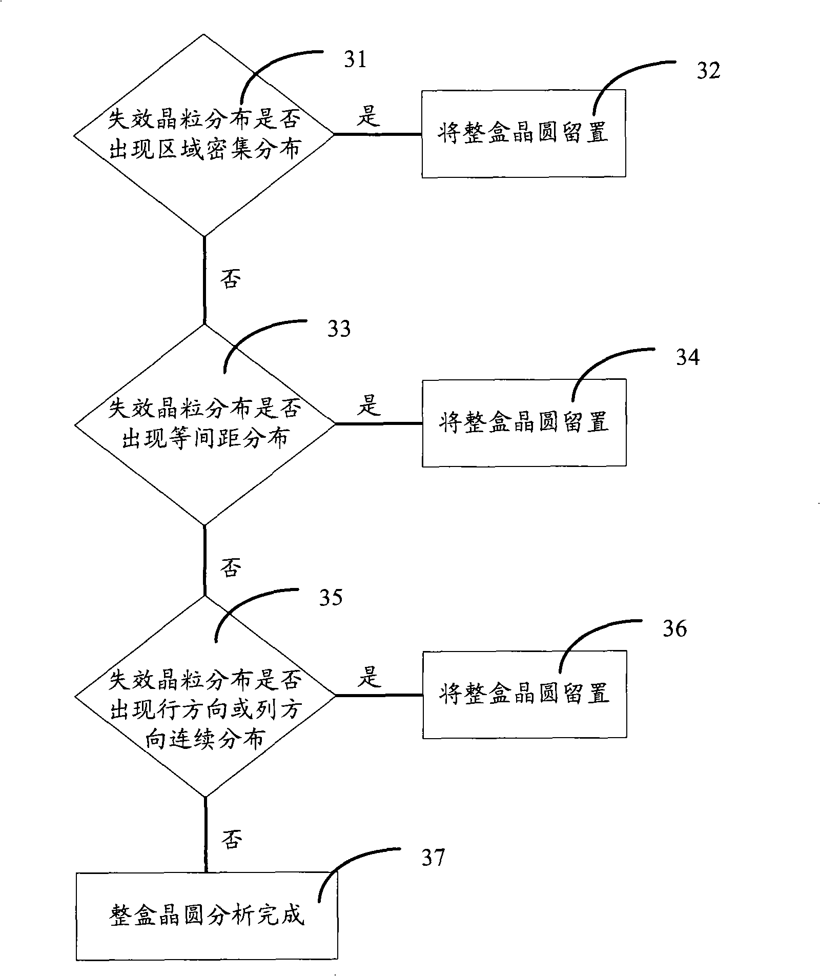
[0036] The wafer quality analysis method of the present invention is to determine the failure of the wafer by comparing the failure grain distribution of the analyzed wafer with the known failure distribution type and the determined full box wafer retention type and single wafer retention type distribution type, and perform quality analysis according to the failure distribution type.

[0037] refer to figure 1 As shown, the wafer quality analysis method of the present invention comprises the following steps,

[0038] Step 1, determine whether the yield rate of the whole box of wafers is lower than the set value and whether the results under the test items are within the set range. As mentioned above, after a series of wafer yield tests, including the yield test of the whole box of wafers and the yield test of a single wafer, the yield and failure grain distribution results of the whole box of wafers will be obtained As well as yield and failed grain distribution results for...


PUM


Abstract

The invention discloses a method for analyzing the quality of a wafer. The method is as follows: a failure distribution pattern of the wafer is determined through the following judgments and then the quality of the wafer is analyzed according to the failure distribution pattern of the wafer: firstly, judgment is made whether the good product ratio of a whole box of wafers is lower than a set value and whether the result under a test item is within a set range; secondly, judgment is made whether the failure crystal grain distribution condition of the whole box of the wafers under the test item belongs to a known failure distribution pattern; thirdly, judgment is made whether a determined retention pattern of the whole box of the wafers occurs during the process of failure crystal grain distribution of the whole box of the wafers under the test item; fourthly, judgment is made whether a determined retention pattern of a single wafer occurs during the process of failure crystal grain distribution of the single wafer. The method for analyzing the quality of the wafer is objective and short in analysis time.

Description

technical field [0001] The invention relates to a method and a device for analyzing wafer quality according to wafer quality detection results. Background technique [0002] Currently, wafer fabrication processes require high levels of precision in process control, equipment operation, and material fabrication. One mistake could result in the complete scrapping of the wafer. Wafer and process quality assessments are made through extensive testing and measurements throughout the process. Among them, the wafer yield rate is a more important indicator to measure whether the performance of the produced wafer is reliable. The wafer yield rate is constrained by many aspects, for example, wafer breakage and bending, process variation, process process defects and photolithography mask defects will all have an impact on the wafer yield rate. In order to ensure the performance of the wafers that are finally provided to customers, it is necessary to perform quality analysis on the t...

Claims


Application Information

Patent Timeline
Patent Type & Authority Applications(China)
IPC IPC(8): H01L21/66
Inventor 林光启张霞峰李琛
Owner SEMICON MFG INT (SHANGHAI) CORP
Learn More