Method for processing printed circuit board

A technology for printed circuit boards and processing methods, which is applied to the formation of electrical connection of printed components, multi-layer circuit manufacturing, etc. The effect of uniform metal layer and improved efficiency

Inactive Publication Date: 2008-10-29
苏州市惠利华电子有限公司
View PDF0 Cites 21 Cited by
  • Summary
  • Abstract
  • Description
  • Claims
  • Application Information

AI Technical Summary

Problems solved by technology

However, the consequences of this operation are that the processing cost of the circuit board is high, the electrodeposition process is complicated, the requirements for the electrodeposition equipment are high, and quality defects are prone to occur, which will affect the subsequent signal transmission.

Method used


Image

  • Method for processing printed circuit board
  • Method for processing printed circuit board
  • Method for processing printed circuit board

Examples


Embodiment Construction

[0026] The invention discloses a processing method of a printed circuit board, and the processing steps of a preferred embodiment thereof will be introduced below with reference to the accompanying drawings.

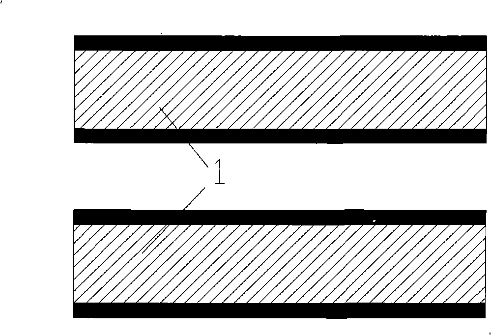
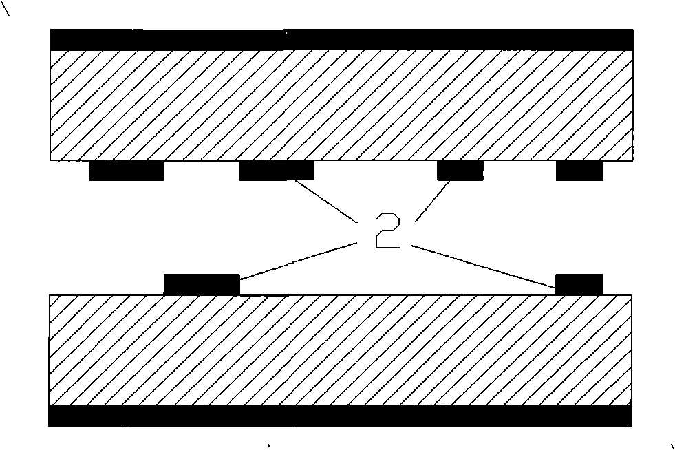
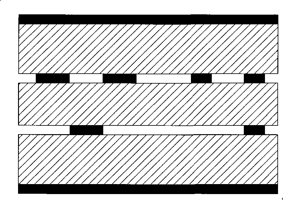
[0027] Such as Figure 1b , first choose two double-sided insulating substrates 1; Figure 2b , using mechanical drilling to process and form through-holes 4 on a single insulating substrate; for example Figure 3b , electrodeposit copper 5 in the through hole of the insulating substrate; as Figure 4b , processing and forming lines 2 on the opposite surfaces of the two substrates; for example Figure 5b , place a new insulating substrate in the middle of the two substrates for lamination processing to form an integral multilayer printed circuit board; such as Figure 6b , using mechanical drilling to process and form the through hole 4 on the multi-layer printed circuit board; for example Figure 7b , electrodepositing copper 5 in the through-hole of the multilayer ...


PUM


Abstract

The invention provides a circuit board processing method for a printed wire, which is used for manufacturing a precision printing blind-hole circuit board and is characterized in that: the conventional double-sided printed board technology is applied to the multi-layer blind-hole board manufacturing completed by utilizing mechanical drilling; a mechanical drilling through-hole method is mainly adopted to divide the multi-layer blind hole board into a plurality of conventional double-sided boards for finishing the manufacturing; and the through-hole method solves the problem of the bad copperplating of the bind-holes which occurs in the process of electrodeposition; the procedure of the method differs from the blind-hole board manufactured by laser drilling at a certain extent and is completed by adopting a part-dividing method; the method can be applied to the technique for manufacturing the blind-hole board with over four layers. The method can greatly reduce production cost and prevent quality defects brought by using the laser drilling to manufacture the blind-hole board.

Description

technical field [0001] The invention relates to a novel processing method of a printed circuit board, in particular to a printed circuit board with multilayer wiring. Background technique [0002] At present, double-sided printed circuit boards are completed by mechanical drilling, and multilayer circuit boards are processed by laser drilling. The reason is that the most important link in the processing of multilayer circuit boards is the processing of blind holes, and the blind holes will be in contact with the wiring on the printed circuit board, and the quality of the processing will directly affect the current on the circuit. Therefore, the processing of blind holes is currently done by laser drilling to complete the interlayer wiring conduction. [0003] Combine below Figures 1a-7a Let's briefly describe the current processing procedures of multilayer circuit boards. Such as Figure 1a , first choose two double-sided insulating substrates 1; Figure 2a , processing...

Claims


Application Information

Patent Timeline
Patent Type & Authority Applications(China)
IPC IPC(8): H05K3/46H05K3/42
Inventor 陈卫芳
Owner 苏州市惠利华电子有限公司
Why Eureka
Try Eureka