
IC testing methods and apparatus

A technology for testing circuits and test patterns, applied in the direction of measuring electricity, measuring devices, measuring electrical variables, etc.

Inactive Publication Date: 2008-11-05
NXP BV
View PDF0 Cites 11 Cited by
  • Summary
  • Abstract
  • Description
  • Claims
  • Application Information

AI Technical Summary

Problems solved by technology

A problem with this approach is that different bypass configurations must be tested for proper functioning as part of the overall testing process

Method used


Image

  • IC testing methods and apparatus
  • IC testing methods and apparatus
  • IC testing methods and apparatus

Examples


Embodiment Construction

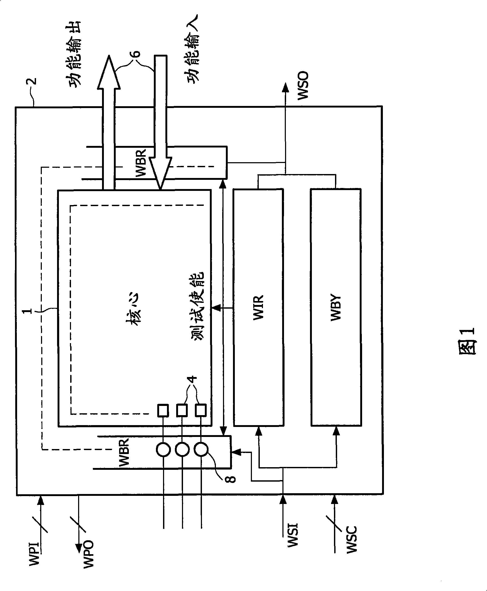
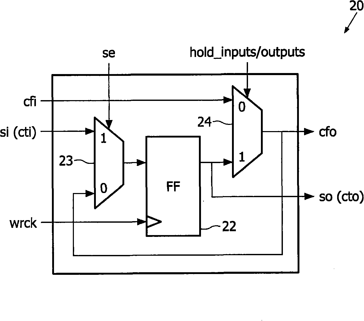
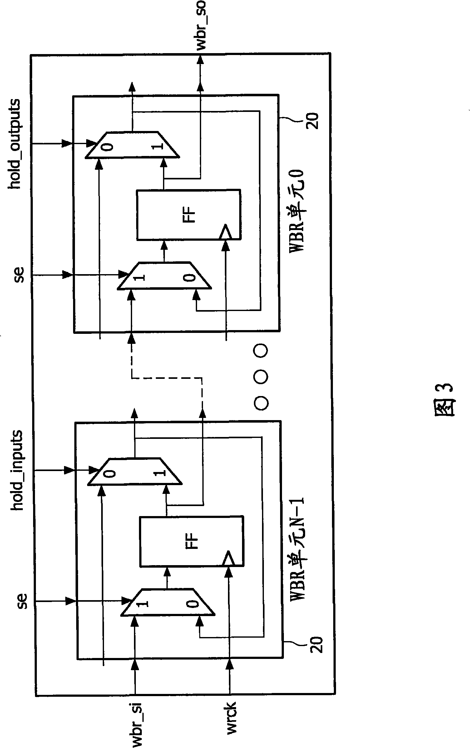
[0064] The example of the invention described below provides an encapsulator architecture in which WBR units are configured in groups in parallel to support reception of parallel data from parallel encapsulator ports.

[0065] A scan chain segment is defined between each serial input and a respective serial output, the scan chain segment comprising a cell set of shift register circuits, a core scan chain portion, a first bypass path bypassing the core scan chain portion, and A second bypass path bypassing the group of shift register circuit cells. This structure enables data to be loaded in parallel to the core scan chains, or to the shift register (WBR). In addition, each scan chain segment has a series latch element, which provides additional test performance. In particular, data shifting between these latch elements can be used to test bypass paths when executing internal or external modes. Therefore, such testing can be performed as part of a single ATPG process.

[006...


PUM


Abstract

A testing circuit has scan chain segments (62,64,60) defined between parallel inputs (wpi[0]...wpi[N-1]) and respective parallel outputs (wpo[0]...wpo[N-1]). The scan chain segments comprise a bank (62) of cells of a shift register circuit, a core scan chain portion (62), a first bypass path around the core scan chain portion (62) and a second bypass path around the bank (60) of cells of the shift register circuit. This architecture enables loading of data in parallel into the core scan chain, or into the shift register (WBR). In addition, each scan chain segment also has a series latching element (80), and this provides additional testing capability. In particular, the shifting of data between the latching elements (80) can be used to test the bypass paths while the internal or external mode testing is being carried out. This testing can thus be part of a single ATPG procedure.

Description

technical field [0001] The present invention generally relates to semiconductor integrated circuit testing, and in particular relates to a core testing method and equipment. Background technique [0002] One conventional testing technique used in the testing of semiconductor integrated circuits (ICs) is the scan testing technique. The technique essentially involves applying a test pattern (called a "vector") to the pins of a device package and monitoring the output response for a specific time, depending on the device's clock speed. A set of test vectors is used to enable the behavior of the device under test to be determined. These vectors are designed to be able to detect manufacturing defects in the device. [0003] As the number of transistors used in integrated circuits increases, the ability to reuse integrated circuit designs becomes increasingly important. An important issue with reusing design functionality (called "cores") is the ability to test these cores with...

Claims


Application Information

Patent Timeline
IPC IPC(8): G01R31/3185
CPCG01R31/318563
Inventor 汤姆·瓦叶尔斯理查德·莫雷
Owner NXP BV
Learn More