Laser processing device

A technology of laser processing and laser beams, which is used in fine work equipment, metal processing, stone processing equipment, etc., can solve the problem of increasing the number of times of irradiating laser beams, and achieve the effect of improving productivity

Inactive Publication Date: 2008-11-26
DISCO CORP
View PDF1 Cites 12 Cited by
  • Summary
  • Abstract
  • Description
  • Claims
  • Application Information

AI Technical Summary

Problems solved by technology

[0005] However, due to the miniaturization of devices, when the number of devices formed on a wafer increases, the num

Method used


Image

  • Laser processing device
  • Laser processing device
  • Laser processing device

Examples


Example Embodiment

[0028] Hereinafter, preferred embodiments of the laser processing apparatus constructed according to the present invention will be described in more detail with reference to the accompanying drawings.

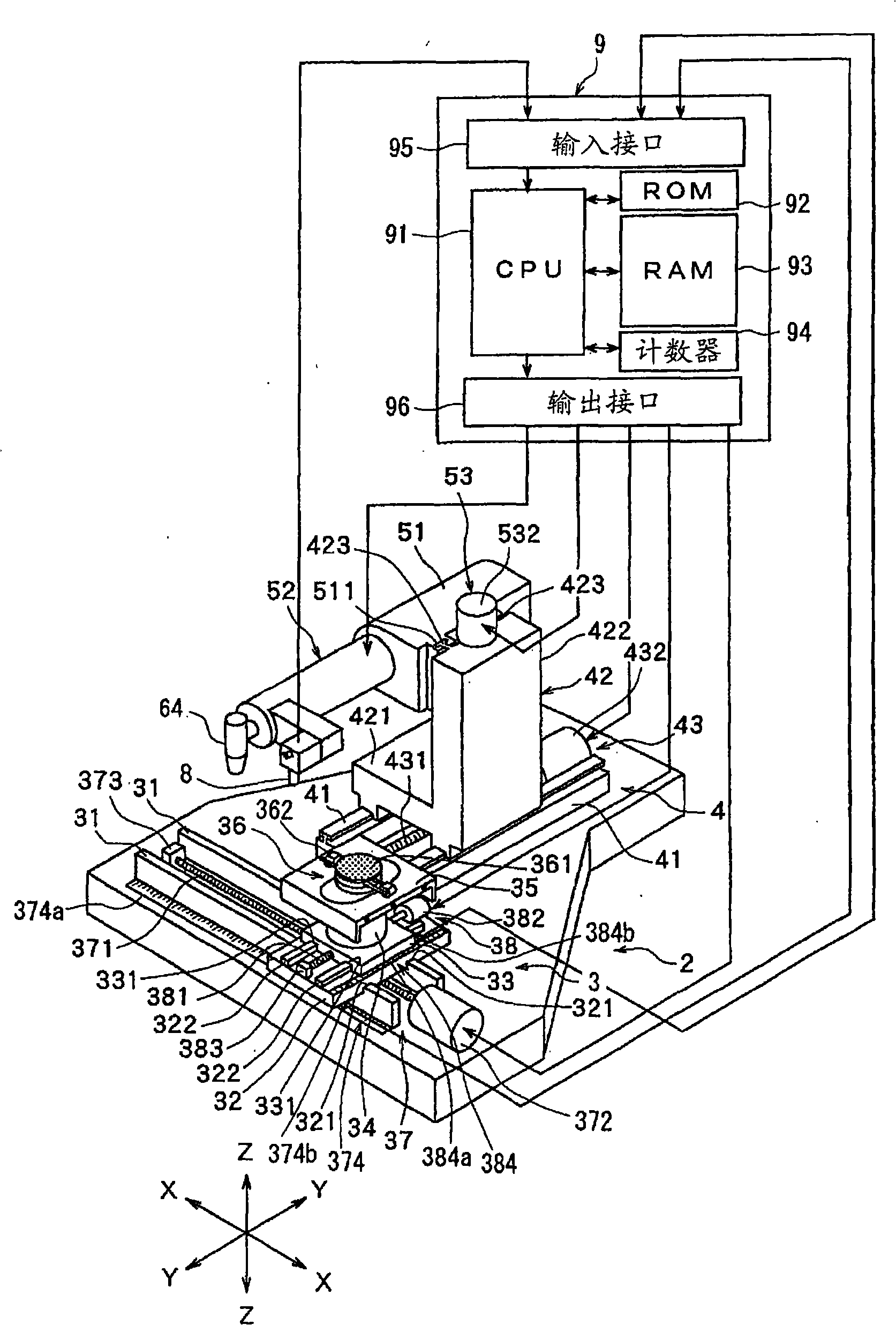
[0029] in figure 1 In the figure, a perspective view of a laser processing apparatus constructed according to the present invention is shown. figure 1 The laser processing device shown has: a stationary base 2; a chuck table mechanism 3, which is arranged on the stationary base 2 in a manner capable of moving along the processing feed direction (X-axis direction) indicated by the arrow X, and To hold the workpiece; the laser beam irradiation unit support mechanism 4, which can be along with the direction indicated by the arrow X (X-axis direction) at right angles to the indexing feed direction indicated by the arrow Y (Y-axis direction) The moving method is arranged on the stationary base 2; and the laser beam irradiation unit 5 is arranged on the laser beam unit supporting mecha...


PUM


Abstract

The invention provides a laser processing device capable of simultaneously applying laser processing along two separating channels. The laser processing device includes: a chuck worktable; a laser beam irradiation unit for irradiation of the laser beam; and a processing giving unit for relatively processing the chuck worktable and the laser beam irradiation unit, wherein the laser beam irradiation unit includes: a laser beam oscillation section; a beam splitter adapted to split the laser beam into a first laser beam and a second laser beam; a condenser lens adapted to condense the first and second laser beams; a prism adapted to lead the first and second laser beams to the condenser lens; a first angle-changing mirror disposed on a first optical path adapted to lead the first laser beam to the prism; a second angle-changing mirror disposed on a second optical path adapted to lead the second laser beam to the prism; and a lamda/2 wave plate disposed on the first or second optical paths to allow direction of one of polarization planes of the first and second laser beams to be aligned with that of the other polarization plane.

Description

technical field [0001] The present invention relates to a laser processing device for performing laser processing along a lane formed on a wafer such as a semiconductor wafer. Background technique [0002] In the manufacturing process of semiconductor devices, on the surface of a roughly disc-shaped semiconductor wafer, a plurality of regions are divided by dividing lines called streets arranged in a grid pattern, and ICs are formed on the divided regions. (Integrated Circuit: integrated circuit), LSI (large scale integration: large scale integrated circuit) and other devices. Then, by cutting the semiconductor wafer along the lanes, the regions where the devices are formed are divided to manufacture individual devices. In addition, optical device wafers in which light-receiving elements such as photodiodes and light-emitting elements such as laser diodes are stacked on the surface of a sapphire substrate or a silicon carbide (SiC) substrate are also cut along the lanes to ...

Claims


Application Information

Patent Timeline
IPC IPC(8): B23K26/067B23K26/073G02B27/09G02B17/08B28D5/00
CPCB23K26/041B23K26/38B23K26/0676B23K26/0853B23K26/067B23K26/0884B23K26/4075B23K2201/40B23K26/0604B23K26/042B23K26/40B23K2101/40B23K2103/50
Inventor 能丸圭司星野仁志山口浩司
Owner DISCO CORP
Why Eureka
Try Eureka