Appearance inspecting device

A technology of appearance inspection device and camera device, which is applied to measuring devices, radiation control devices, televisions, etc., can solve the problem of resolution reduction, and achieve the effect of suppressing the increase and suppressing the amount of processing

Inactive Publication Date: 2008-12-17
SHIBAURA MECHATRONICS CORP
View PDF2 Cites 3 Cited by
  • Summary
  • Abstract
  • Description
  • Claims
  • Application Information

AI Technical Summary

Problems solved by technology

Therefore, it is considered that by reducing the resolution of each line sensor, the increase in its processing capacity can be suppressed, but this will directly lead to a decrease in the resolution of defect detection such as scratches on the surface of the object to be inspected.

Method used


Image

  • Appearance inspecting device
  • Appearance inspecting device
  • Appearance inspecting device

Examples


Embodiment Construction

[0042] Embodiments of the present invention will be described below with reference to the drawings.

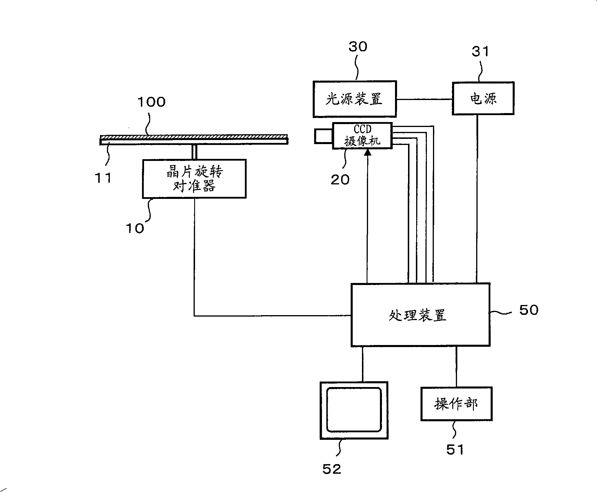
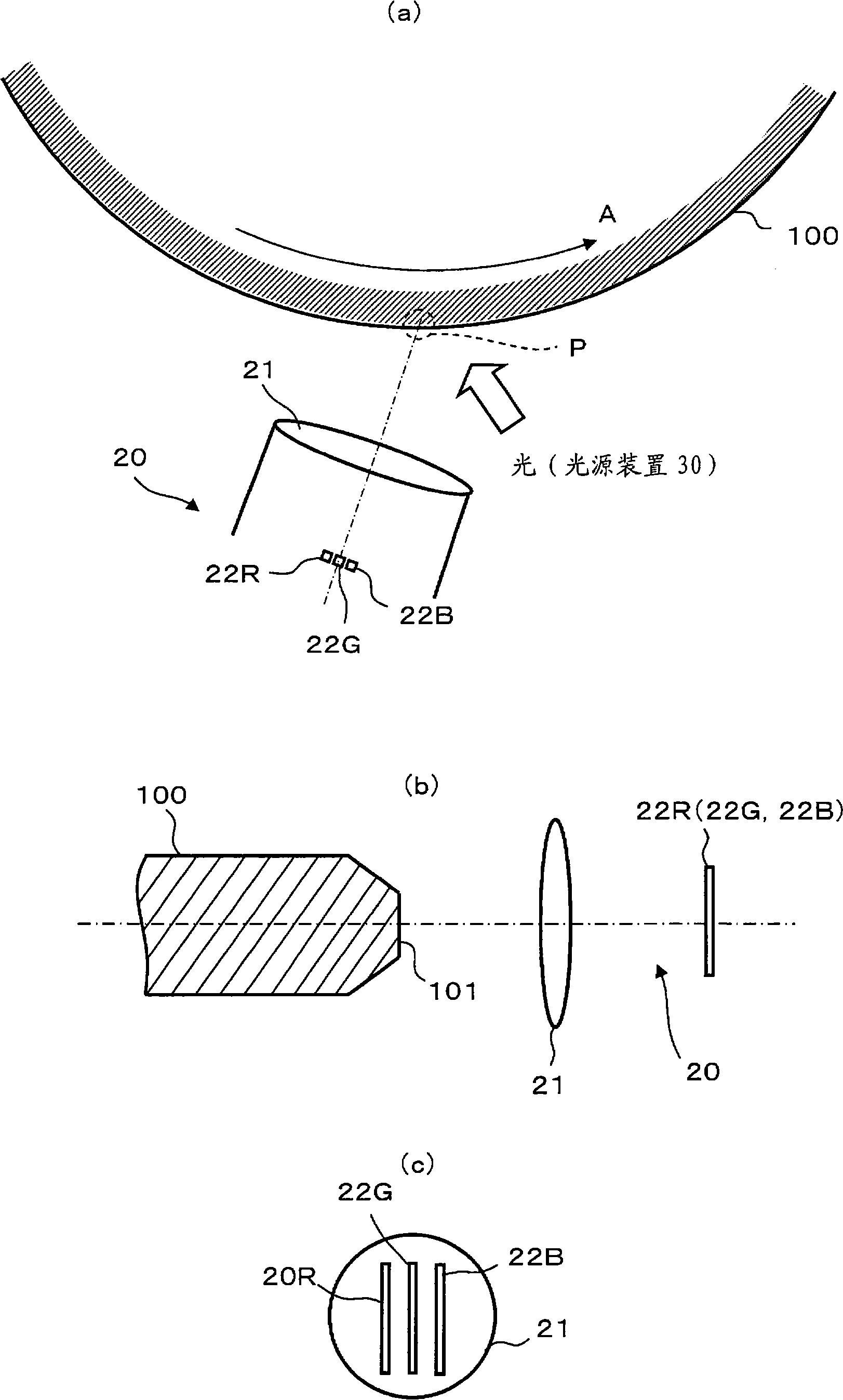
[0043] An appearance inspection device according to an embodiment of the present invention is based on figure 1 composition shown. This appearance inspection device inspects the appearance of the outer peripheral end surface of a semiconductor wafer.

[0044] exist figure 1 Among them, the visual inspection apparatus has a wafer rotational aligner 10 . A semiconductor wafer 100 to be inspected is set on a turntable 11 rotated by a wafer rotational aligner 10 . In addition, a CCD camera 20 constituting the imaging device is provided in a predetermined positional relationship with respect to the outer peripheral end face of the semiconductor wafer 100 placed on the turntable 11, and the light source device 30 that emits diffused light by supplying power from the power supply 31, The peripheral end surface of the semiconductor wafer 100 within the imaging range of the CCD cam...


PUM


Abstract

An appearance inspecting device for detecting a defect such as a scratch in the surface of an object to be inspected with an adequate resolution and judging the formed state of a film on the surface of the object while suppressing an increase of the throughput to an irreducible minimum. An appearance inspecting device comprises an imaging unit (20) having line sensors (22R, 22G, 22B) having different color sensitivities and a processing unit (50). The processing unit (50) has pixel data acquiring means (S14) for acquiring pixel gray-scale data with a first pixel density from the gray-scale signal from a reference line sensor and acquiring pixel gray-scale data with a second pixel density lower than the first pixel density from the gray-scale signals from the line sensors other than the reference line sensor. Information representing the state of the surface of the object is created from the pixel gray-scale data acquired with the first pixel density and that acquired with the second pixel density.

Description

technical field [0001] The present invention relates to an appearance inspection device for inspecting the appearance of an object surface to be inspected, such as an outer peripheral end surface of a semiconductor wafer. Background technique [0002] Conventionally, an inspection device (appearance inspection device) for detecting defects on the outer peripheral end surface of a semiconductor wafer has been proposed (for example, Patent Document 1). The inspection apparatus generates information indicating the state of the outer peripheral end surface of the semiconductor wafer, for example, image information representing the outer peripheral end surface, based on a density signal for each pixel obtained when the outer peripheral end surface of the semiconductor wafer to be inspected is scanned by a line sensor, and information indicating defects, scratches, foreign matter, etc. on the outer peripheral end face. According to such an inspection device, it is possible to det...

Claims


Application Information

Patent Timeline
Patent Type & Authority Applications(China)
IPC IPC(8): G01N21/956H01L21/66H04N5/335
CPCG01N21/9503G01N21/9501H04N23/84H01L27/146
Inventor 林义典森秀树
Owner SHIBAURA MECHATRONICS CORP
Why Eureka
Try Eureka