


Quick Research
Generate reliable direction feasibility study reports for your R&D in just a few steps.

Technical Q&A
Discover and master advanced knowledge NOW. Basics, ideas, possibilities, all at once.

Find Solutions
As an expert in R&D theories, this can generate solutions to your technical problems instantly.

Evaluate Feasibility
Analyze your overall solution with one click, know your potential R&D risks in advance.

Monitor Landscape
Get weekly tech updates, stay abreast of the latest tech innovations and key insights.
Lateral bipolar transistor and method of production
A bipolar transistor, horizontal technology, applied in semiconductor/solid-state device manufacturing, semiconductor devices, electrical components, etc., can solve problems such as increasing resistance
- Summary
- Abstract
- Description
- Claims
- Application Information
AI Technical Summary
Problems solved by technology
Method used
Image

Examples
Embodiment Construction
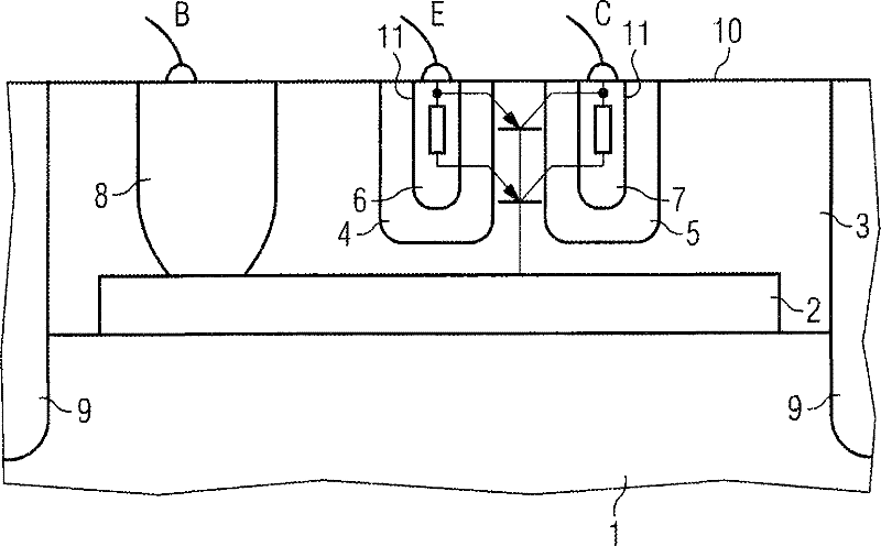
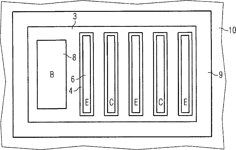
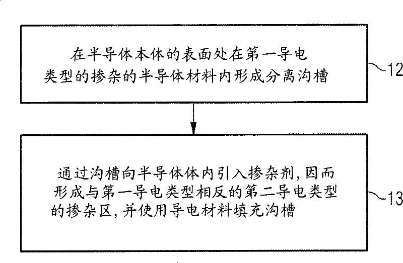
[0013] figure 1 A cross-section of an embodiment of a lateral bipolar transistor is shown. The transistor structure is located at the surface 10 of the semiconductor body 1 . The buried layer 2 of the first conductivity type can be arranged in a doped well 3 which is also of the first conductivity type but has a lower doping compared to the buried layer 2 . Separate doped regions 4 , 5 of a second conductivity type opposite to the first conductivity type are arranged in the well 3 . The conductive material 6, 7 is arranged in the trench 11 in contact with the doped regions 4, 5, so that one doped region 4 with the corresponding conductive material 6 forms an emitter, and the other doped region 5 with the corresponding conductive material 7 Forms the collector of the lateral bipolar transistor. Between the doped regions 4, 5 there is a doping material of the well 3 of opposite conductivity type. Therefore, there is a pn junction between the doped region and the well.
[00...
PUM
 Abstract
Description
Claims
Application Information
 - R&D Engineer
- R&D Manager
- IP Professional
- Industry Leading Data Capabilities
- Powerful AI technology
- Patent DNA Extraction
Browse by: Latest US Patents, China's latest patents, Technical Efficacy Thesaurus, Application Domain, Technology Topic, Popular Technical Reports.
© 2024 PatSnap. All rights reserved.Legal|Privacy policy|Modern Slavery Act Transparency Statement|Sitemap|About US| Contact US: help@patsnap.com