Erasing method and apparatus of memory block

A storage block, erasing times technology, applied in the field of flash memory management, can solve problems such as increased wear, low utilization, high erasing times, etc., to achieve the effect of eliminating negative effects

Inactive Publication Date: 2009-01-07
HUAZHONG UNIV OF SCI & TECH
View PDF0 Cites 57 Cited by
  • Summary
  • Abstract
  • Description
  • Claims
  • Application Information

AI Technical Summary

Problems solved by technology

[0021] In the above situation, the block with high erasure frequency and low utilization rate may be repeatedl

Method used


Image

  • Erasing method and apparatus of memory block
  • Erasing method and apparatus of memory block
  • Erasing method and apparatus of memory block

Examples


Embodiment Construction

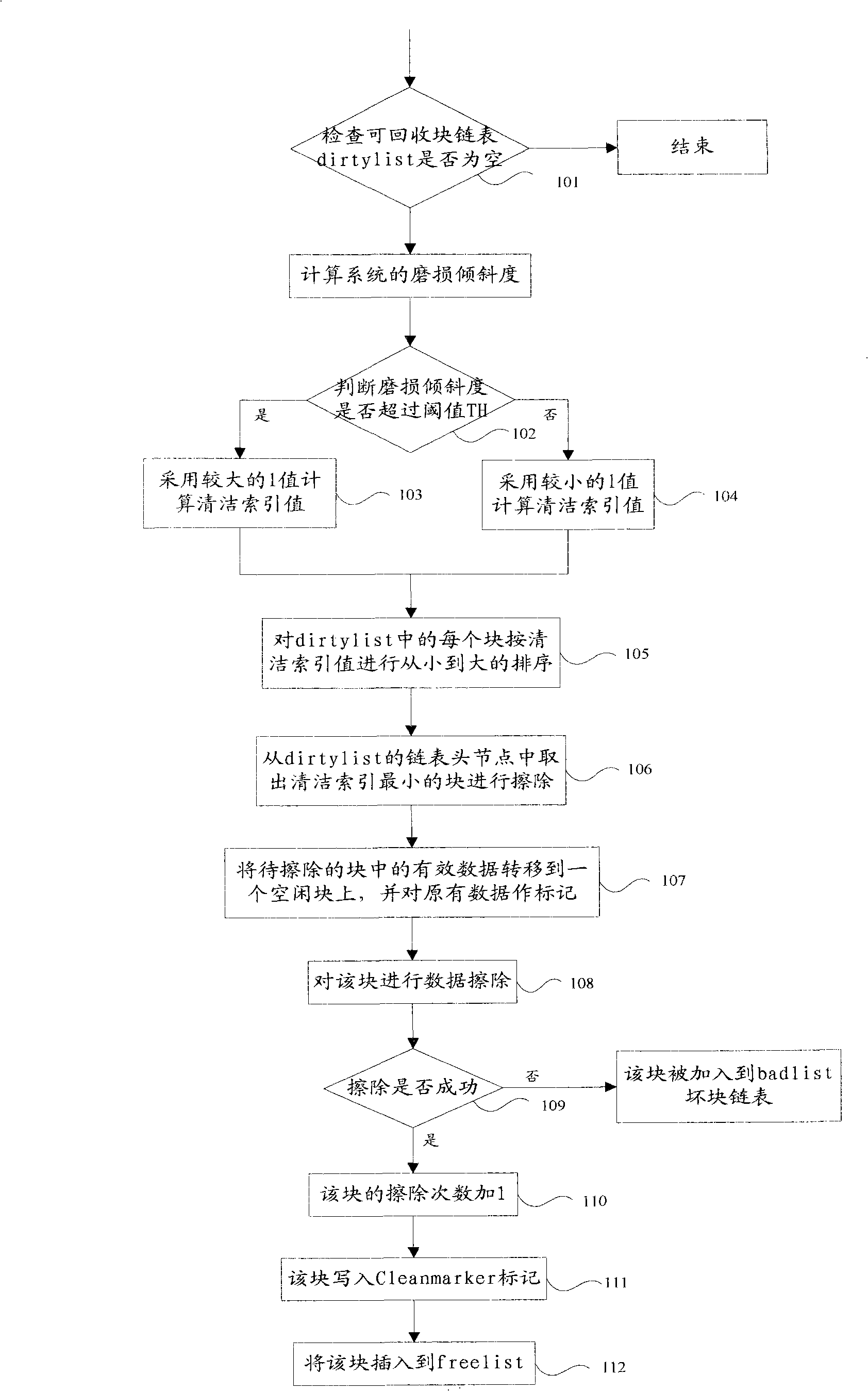
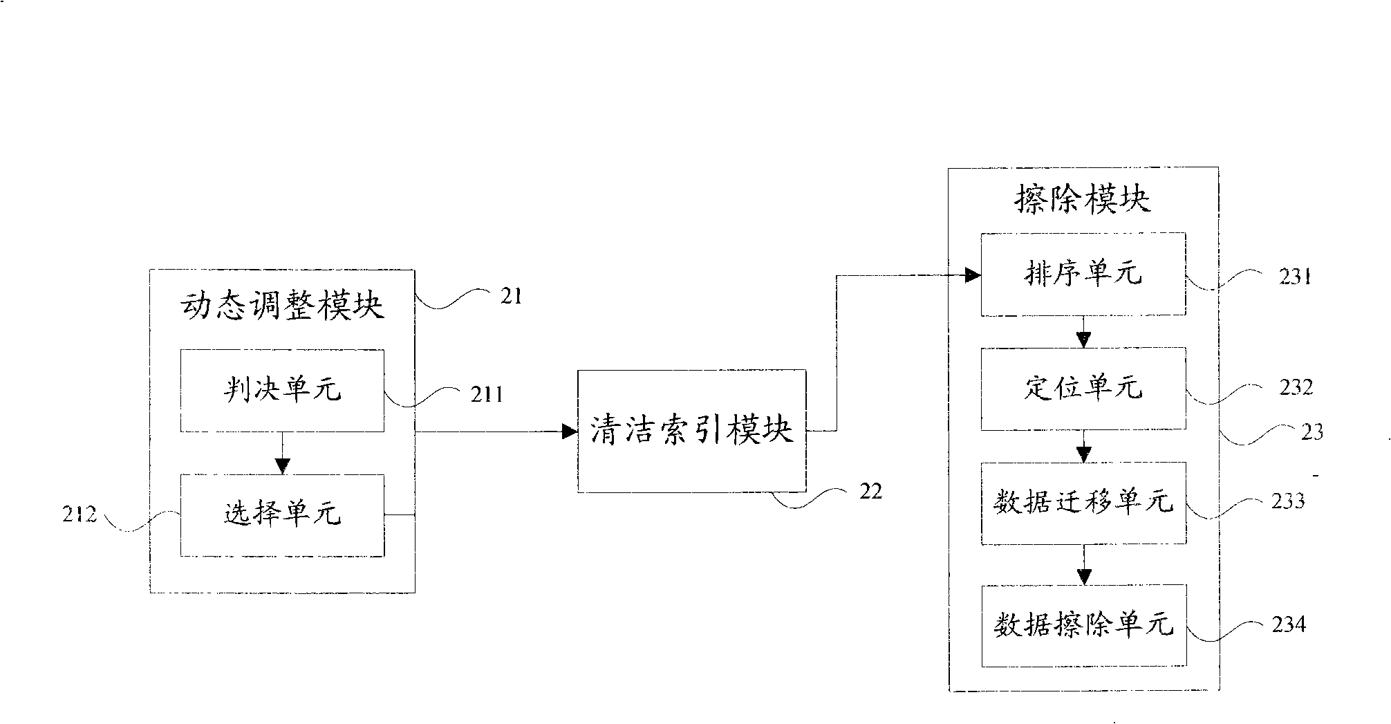
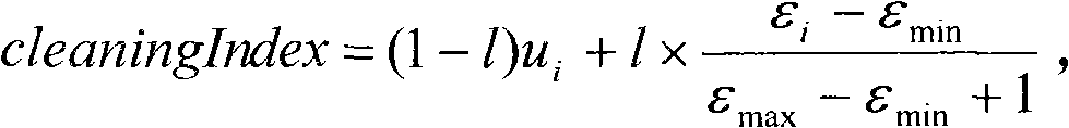
[0033] Due to some flaws inherent in the Kim and Lee algorithm, blocks with low utilization and high erasure counts are selected based on the clean index, resulting in aggravated wear.

[0034] In addition, the regular lower flushness l in the Kim and Lee algorithm is a static value, which simplifies the calculation of its cleaning index value and cannot take into account some special cases. For example, when the chip is erased less often, the recovery efficiency should be improved as much as possible, that is, as much space as possible should be recovered; and when the chip is erased more often, the factor of wear balance should be considered.

[0035] The embodiment of the present invention uses an improved clean index algorithm to well solve some flaws in the clean index calculation method in the Kimand Lee algorithm, which results in blocks with low utilization and high erasure times being selected according to the clean index. The resulting wear aggravates the problem. I...


PUM


Abstract

The invention discloses an erasing method of a memory block, which comprises the steps as follows: tendency between recovery efficiency and wear leveling is dynamically regulated according to degree of wear uniformity of a memory block containing invalid data to acquire a cleanness index value of the memory block, and then the memory block to be erased is determined according to the cleanness index value for data erasing. The invention further discloses an erasing device of the memory block, which comprises a dynamic regulation module, a cleanness index module and an erasing module. By providing a new calculation method of the cleanness index, the invention introduces a new parameter, which causes the wear leveling among blocks to be still effectively calculated when erasing times of the block approximates the erasing limit. Meanwhile, a dynamic regulation method is provided to dynamically regulate the tendency between the recovery efficiency and the wear leveling according to the degree of wear uniformity, thus ensuring that the garbage collection of a flash memory has more balanced performance and adaptive ability.

Description

technical field [0001] The invention relates to the management technology of flash memory, in particular to a memory block erasing method and device. Background technique [0002] Flash memory card (flash memory) is mainly used in smart phones, digital cameras, PDA and other related fields. It consists of two parts: Flash memory chip and memory card control circuit. Among them, the Flash memory chip is the storage entity of the Flash memory card, which is a semiconductor-based memory with the advantages of low power consumption, large capacity, high access speed, no mechanical failure, and non-volatile data. With the rapid growth of the capacity of Flash memory chips, people have put forward higher and higher requirements for the flexibility of data operations, and the management of data storage in Flash memory chips has become an unavoidable problem. [0003] After repeated reading and writing of the flash memory, there will be a large number of file fragments within and b...

Claims


Application Information

Patent Timeline
IPC IPC(8): G11C16/10G06F12/02
CPCG06F12/0246G06F2212/1016G06F2212/7211
Inventor 余鑫吴小龙
Owner HUAZHONG UNIV OF SCI & TECH
Why Eureka
Try Eureka