Clock receiver and correlative semiconductor memory module and emendation method

A storage module and receiver technology, applied in information storage, static memory, digital memory information and other directions, can solve problems affecting clock signal edge, phase offset, etc.

Active Publication Date: 2011-03-16
NAN YA TECH
View PDF0 Cites 0 Cited by
  • Summary
  • Abstract
  • Description
  • Claims
  • Application Information

AI Technical Summary

Problems solved by technology

Therefore, the main clock signals MCLK and MCLK" will have a phase offset, which will affect the margin of the clock signal in the internal circuit.

Method used


Image

  • Clock receiver and correlative semiconductor memory module and emendation method
  • Clock receiver and correlative semiconductor memory module and emendation method
  • Clock receiver and correlative semiconductor memory module and emendation method

Examples


Embodiment Construction

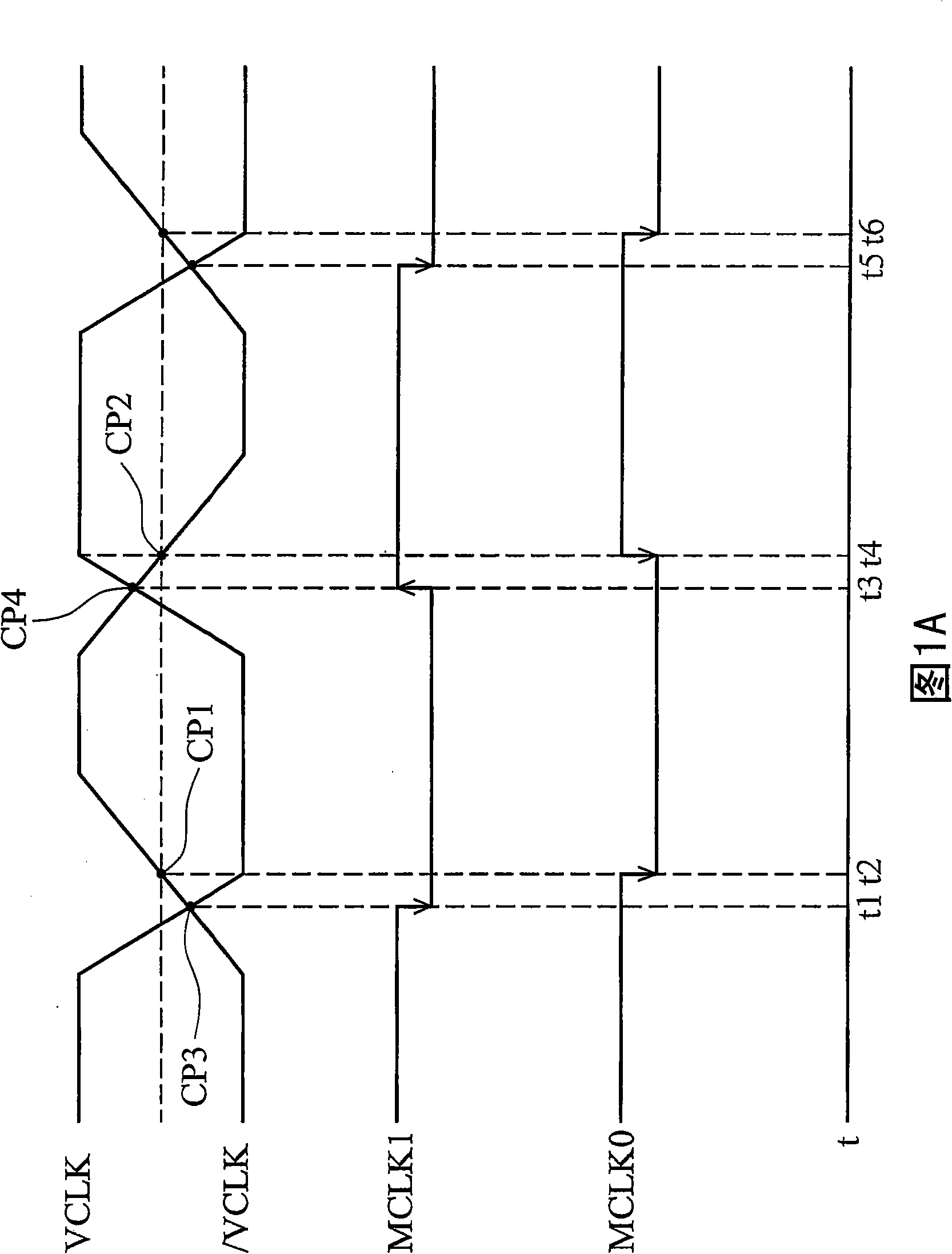
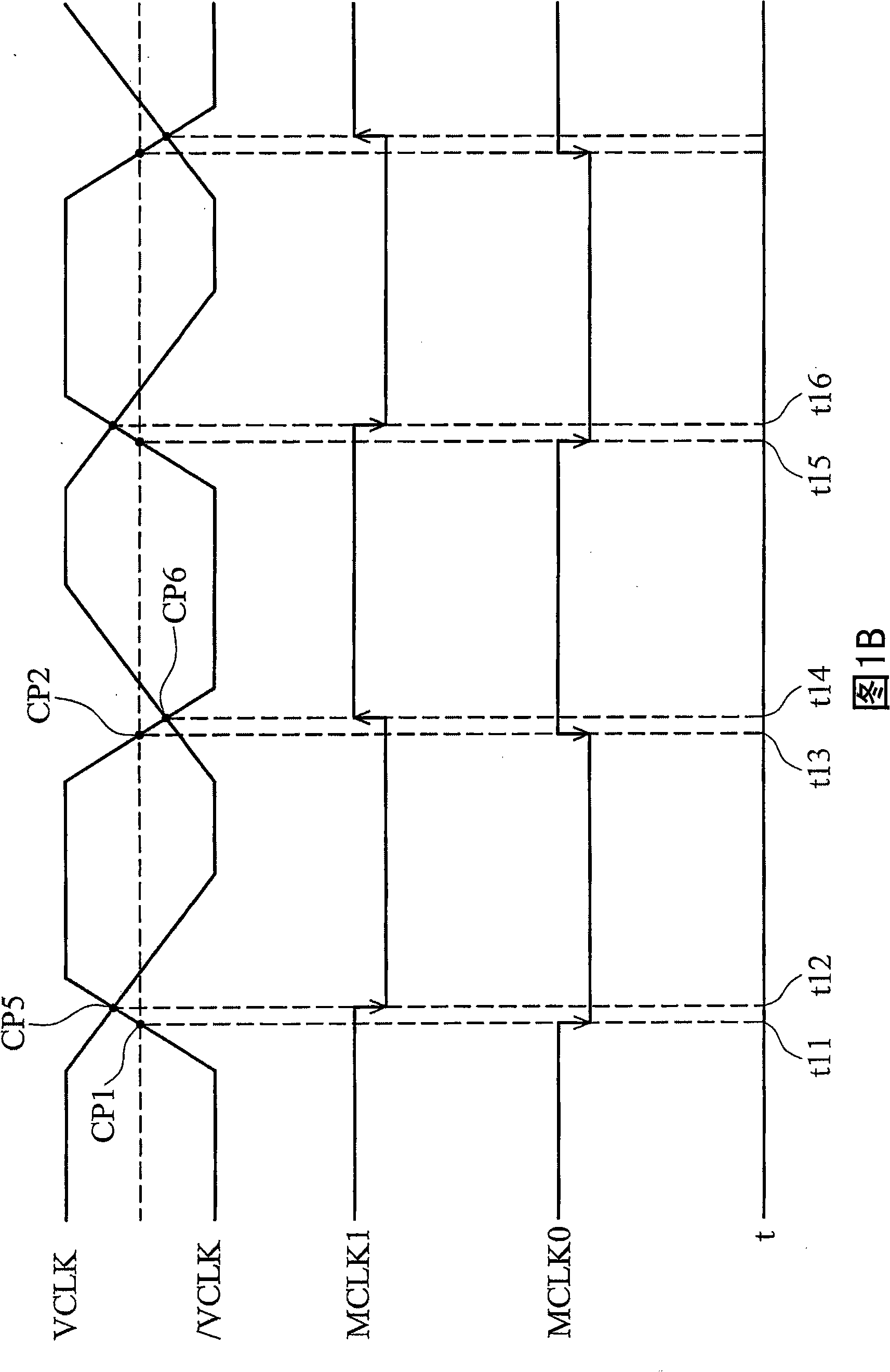
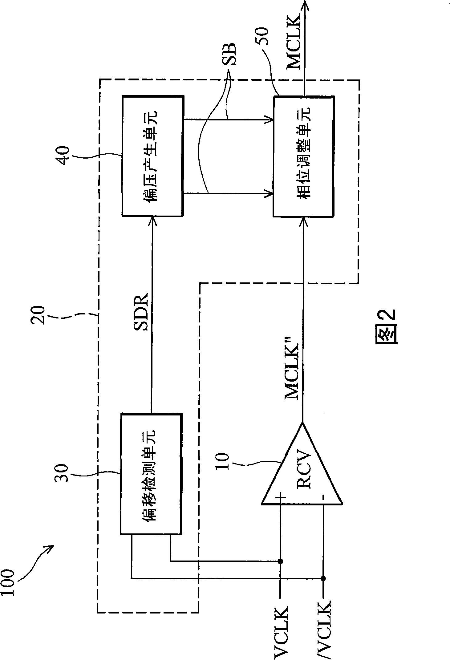
[0041] figure 2 Shown is an embodiment of a clock receiver of the present invention. As shown in the figure, the clock receiver 100 includes: a receiving unit 10 for receiving a complementary clock signal VCLK and / VCLK and generating a clock signal MCLK”; and a correction unit 20 for detecting the clock signal VCLK and / Whether the intersection point of VCLK is shifted, the toggling of the clock signal MCLK" is adjusted so as to output a main clock signal MCLK. The calibration unit 20 includes an offset detection unit 30 , a bias voltage generation unit 40 and a phase adjustment unit 50 . For example, the clock receiver 100 can be disposed in a semiconductor chip, but not limited thereto.

[0042] The receiving unit 10 is used to receive the clock signals VCLK and / VCLK to generate a corresponding clock signal MCLK". For example, the receiving unit 10 can be a receiver, when the level of the clock signal VCLK is higher than the clock signal / VCLK When the level is high, ...


PUM


Abstract

The invention provides a clock receiver and related semiconductor memory module and correction method. The clock receiver comprises: a receiving units, for receiving a pair of complementary clock signal and produce a first clock signal; a correction unit, for detecting if there is a offset for crossing point of complementary clock signal and produce a result then regulating the first clock signal toggling. Crossing point offset resulting from inconsistent work cycle of clock signal VCLK / VCLK can be automatically corrected in the invention, thereby not influencing clock signal margin of internal circuit.

Description

technical field [0001] The present invention relates to semiconductor circuits, in particular to a clock receiver capable of automatically correcting phase shifts caused by inconsistencies in duty cycles of complementary clock signals. Background technique [0002] Generally speaking, a dynamic random access memory (DRAM) will use a receiver to receive a pair of complementary clock signals (such as: VCLK and / VCLK) from an external circuit, thereby generating a main clock signal (such as: MCLK) For internal circuit use. However, due to component mismatch, temperature or other factors, the duty cycles of the complementary clock signals (VCLK and / VCLK) will be inconsistent. [0003] Such as Figure 1A As shown, the duty cycle (duty cycle) of the clock VCLK is greater than the duty cycle of / VCLK, which will cause the two clock signals to generate cross points (cross points) CP3 and CP4 at time t1 and t3 respectively, but not at predetermined time t2 and t4 Intersection poin...

Claims


Application Information

Patent Timeline
Patent Type & Authority Patents(China)
IPC IPC(8): H03L7/00G11C7/22G11C11/4063
Inventor 郑文昌
Owner NAN YA TECH
Why Eureka
Try Eureka